 Bharbour
Old Style or PWM interfaced hobby servos use pulses that vary from about 1.0mS to about 2.0mS wide with a period of about 20mS out to about 50mS. Pre 2.4GHz radios sent the signals for each channel sequentially, followed by a longer "frame" synchronization period. The exact values vary slightly depending on the radio manufacturer and the number of channels that the radio has.
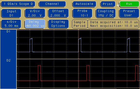
This scope shot shows 3 "frames" of data for 2 channels. The channel signals may or may not be consecutive, depending on which channels are viewed. The order that each channel is sent in the frame is dependent on the manufacturer of the radio. These two channel signals would be from non-adjacent channels with the control inputs approximately centered (1.5mS).
Here is a closer view of one frame of data for 2 channels.
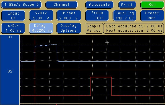
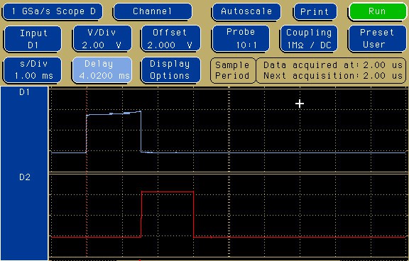
The separation in time between the two non-consecutive channels is apparent here. Here is a shot that corresponds to consecutive channels
When running servos, the channel sequence and spacing is completely irrelevant, as each servo has no knowledge of other channel timing. When you are developing an interface to a microcontroller or other digital system, the spacing becomes important. Since the signals are sequential, is is possible to use a single timer to monitor both signals, but it requires some thinking to get it to work with different radio configurations.
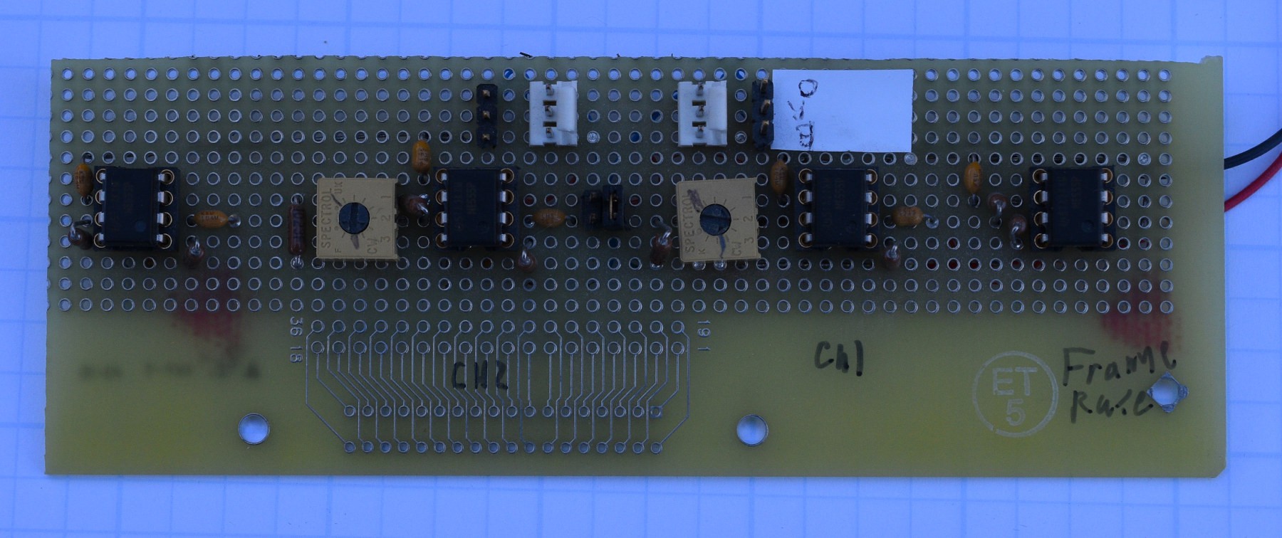
Implementation
Following along on the schematic diagram will help this section make sense.
The frame repetition rate is set by U1. It generates a short negative going pulse every 20mS as a free running oscillator. All of the rest of the 555s are set up in one-shot mode that are triggered off the falling edge of the output of the previous stage. Since the 555 requires the trigger signal to go high again before it times out, the trigger signal is coupled through a capacitor and pulled up by a resistor (channel 1 uses C8 and R7 for this).
Channel 1 (U2) is triggered from the output of U1 and it's output pulse length can be adjusted by turning the knob on R5. R13 is marked DNP (Do Not Place) in the schematic, but putting it in makes the adjustment range of R5 match the desired 1.0 to 2.0mS better. The output of U2 goes up to the servo connectors, to pin 1 of J5 and the trigger input of U4.
U4 generates the interchannel delay for simulating non-sequential channel operation. It provides a fixed delay (2.2mS) after the end of the channel 1 output pulse. It's output goes to pin 3 of J5. The exact delay value is not critical, it's purpose is just to make the rising edge of channel 2 not be adjacent to the falling edge of channel 1.
Jumper J5 is used to select immediate or delayed trigger for channel 2 (U4). Jumpering from pin 1 to 2 makes channel 2 trigger on the falling edge of channel 1 which would model consecutive channel assignment. Jumpering from pin 2 to 3 on J5 causes channel 2 to be triggered after the interchannel delay ends.
Pulse output length for channel 2 (U4) is adjusted with R6. The output of U4 goes to the servo connectors.
Power to the servos is supplied through 0.1 Ohm resistors to allow measuring the current into each servo. One side of a meter or scope input should be connected to TP_REF, and the other side to TP1 or TP2 for channel 1 or 2. The current sensing is done on the + power side of the servo power.
This PCB has connectors for either the old 0.100" cables or the newer JST SHR type connector. One thing to note is that this board is wired for JR / Spectrum servos on the 0.100" connectors, Futaba servos swapped the + and the signal pins (or at least they were in 1998).
Power can be connected to the board through P1, or possibly through a speed control (battery eliminator) on one of the servo channels. Old systems ran on 4 NiCad or NiMH cells, so they ran about 4.8 or 5V. Some newer systems run on a single Li cell for around 3.3V. If you are in doubt about what your servos require, check the data sheet.
As the power supply voltage drops below 5.0V, channel 2 had problems with triggering at low pulse widths on channel 1 with my original design. The problem is R9 and R11, C9 and C15. At low pulse widths on channel 1, C9 and C15 were not discharging enough to trigger the channel 2 input. Changed R9 and R11 out from 3.9K to 2.7K and C9 and C15 from 0.1uF to 0.022uF and the board works fine at 3.3V and 5V now. (12/23/2019)
Here is the original implementation of this project.