 Gerriko IO
Ten years ago, RS232 was a very common interface, but it appears to me that is has become less ubiquitous. As such, I felt that RS232 very much fits within the "Take Flight with Feather" Retro Feather category -- where old tech lives on, but can you design a Feather to interact with it?
I've basically take an existing proven design from Sparkfun Electronics and tweaked it, as explained in the project description.
First we have the RS232 to TTL conversion.
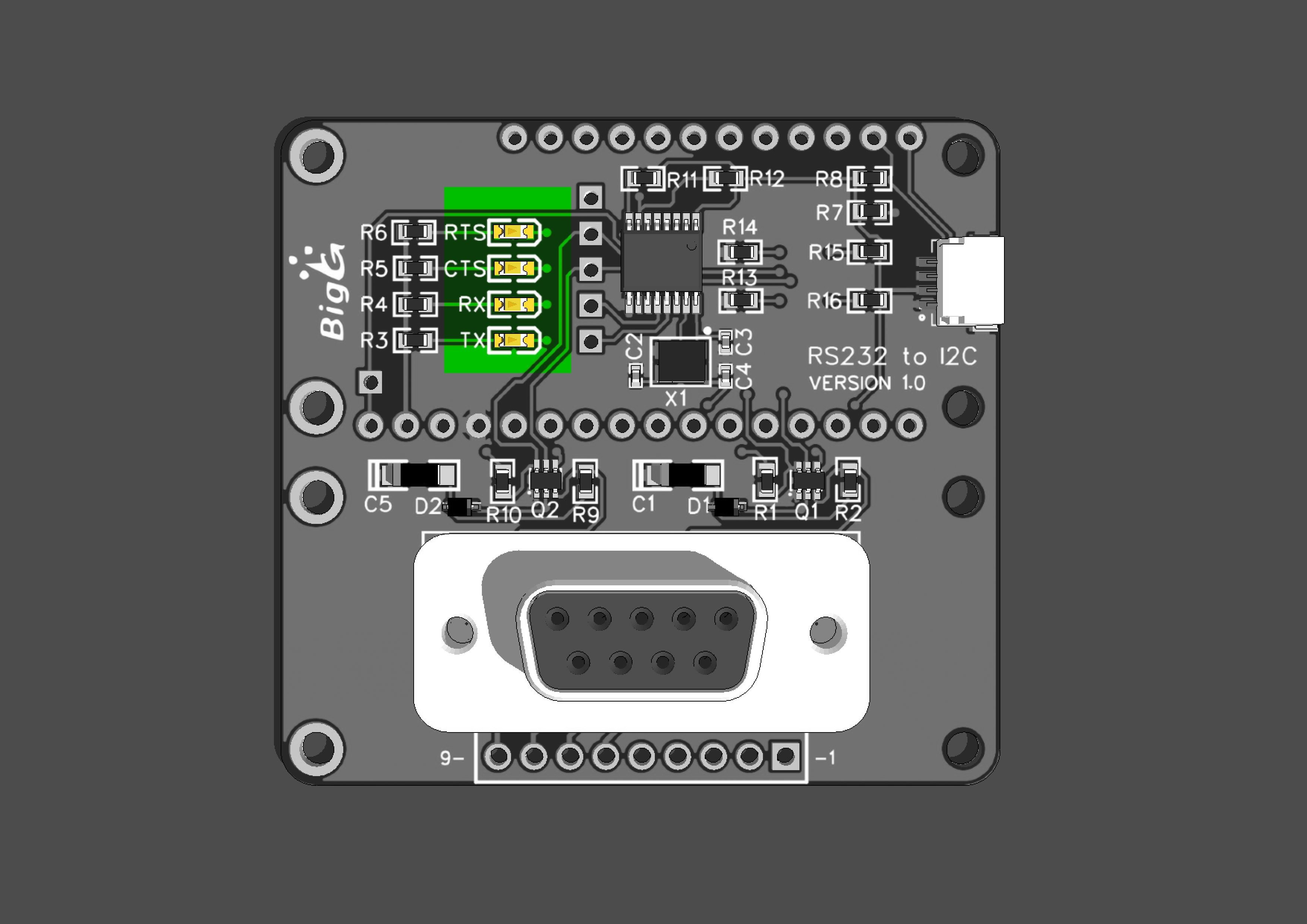
The RS232 to TTL (RX, TX, CTS, & RTS) is handled via this circuit, which is basically a clone of the Sparkfun RS232 Shifter DB9 board design. Details can be found on Sparkfun's GitHub page: https://github.com/sparkfun/RS232_Shifter_SMD
In my case I duplicated the circuit for to handle CTS and RTS too.
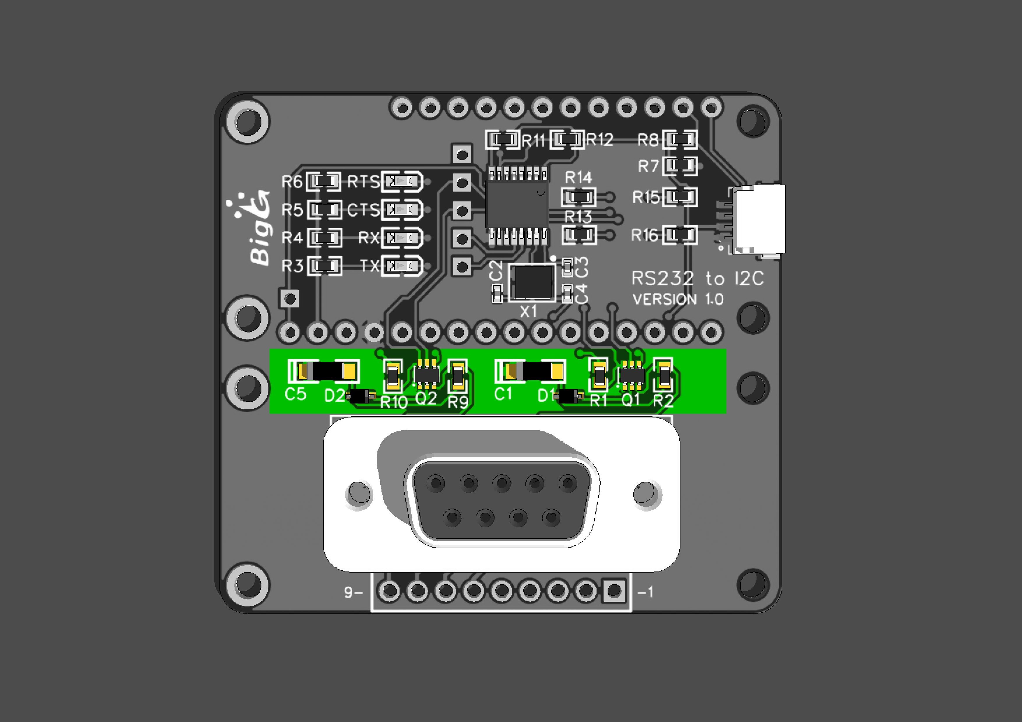
Instead of a righthand DB9 connector I chose to use a straight connector as this free up space for the additional DB9 breakout header pins.
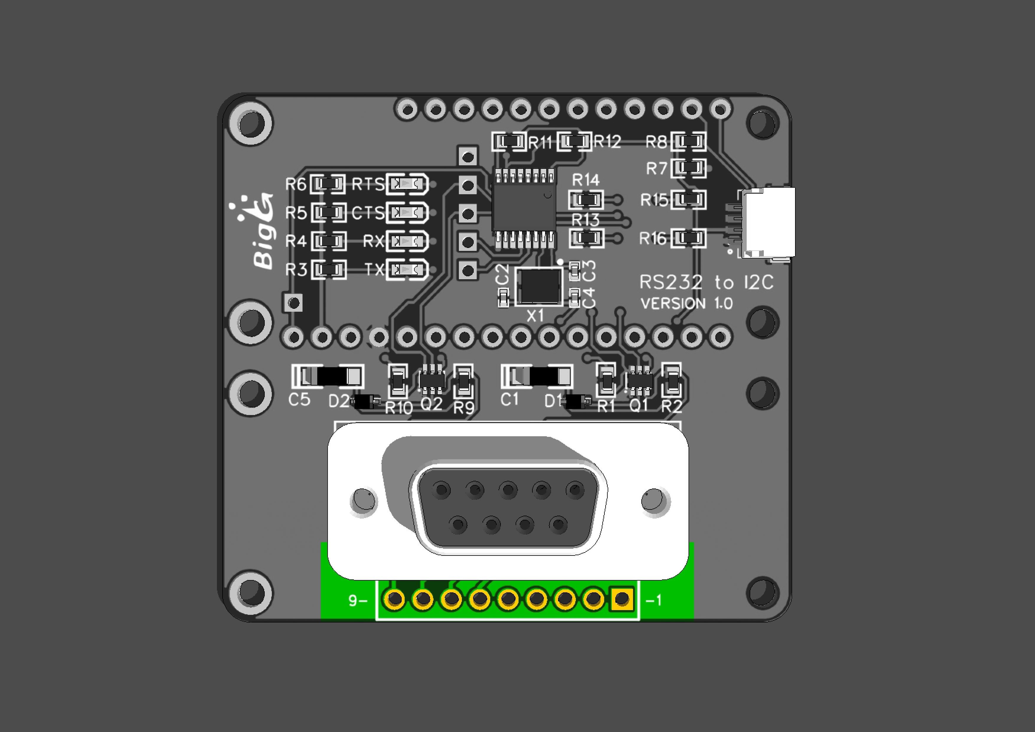
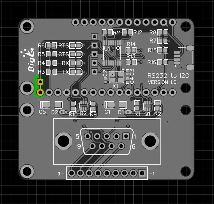
Should a crossover configuration be required for the DB9 pins, this is handled via a solder joints:
The TTL pins are broken out, should you wish to only use UART.
I also included 4 LED's to give you a visual indication of what is happening with UART signals:
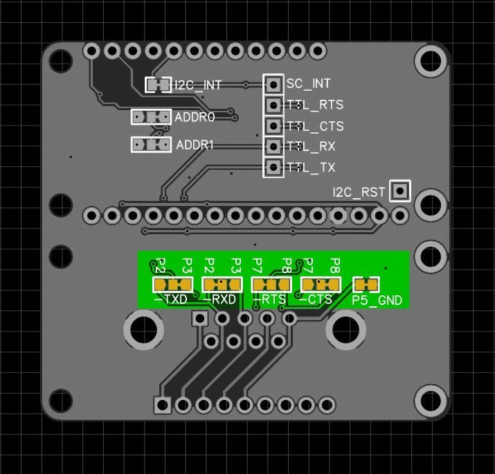
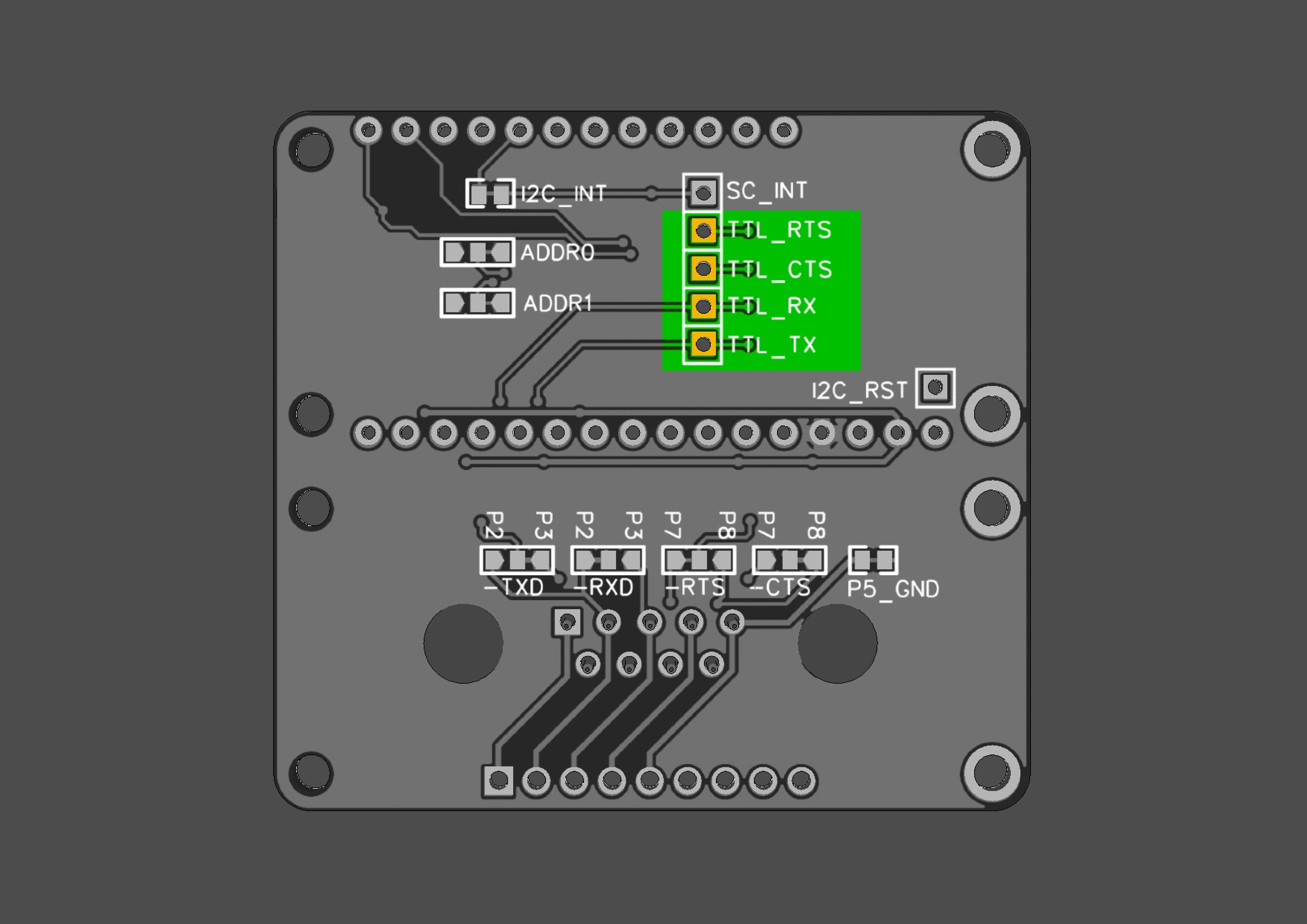
Then we have circuitry to handle the TTL to I2C conversion.
The TTL (UART) to I2C conversion is handled via the components placed here:
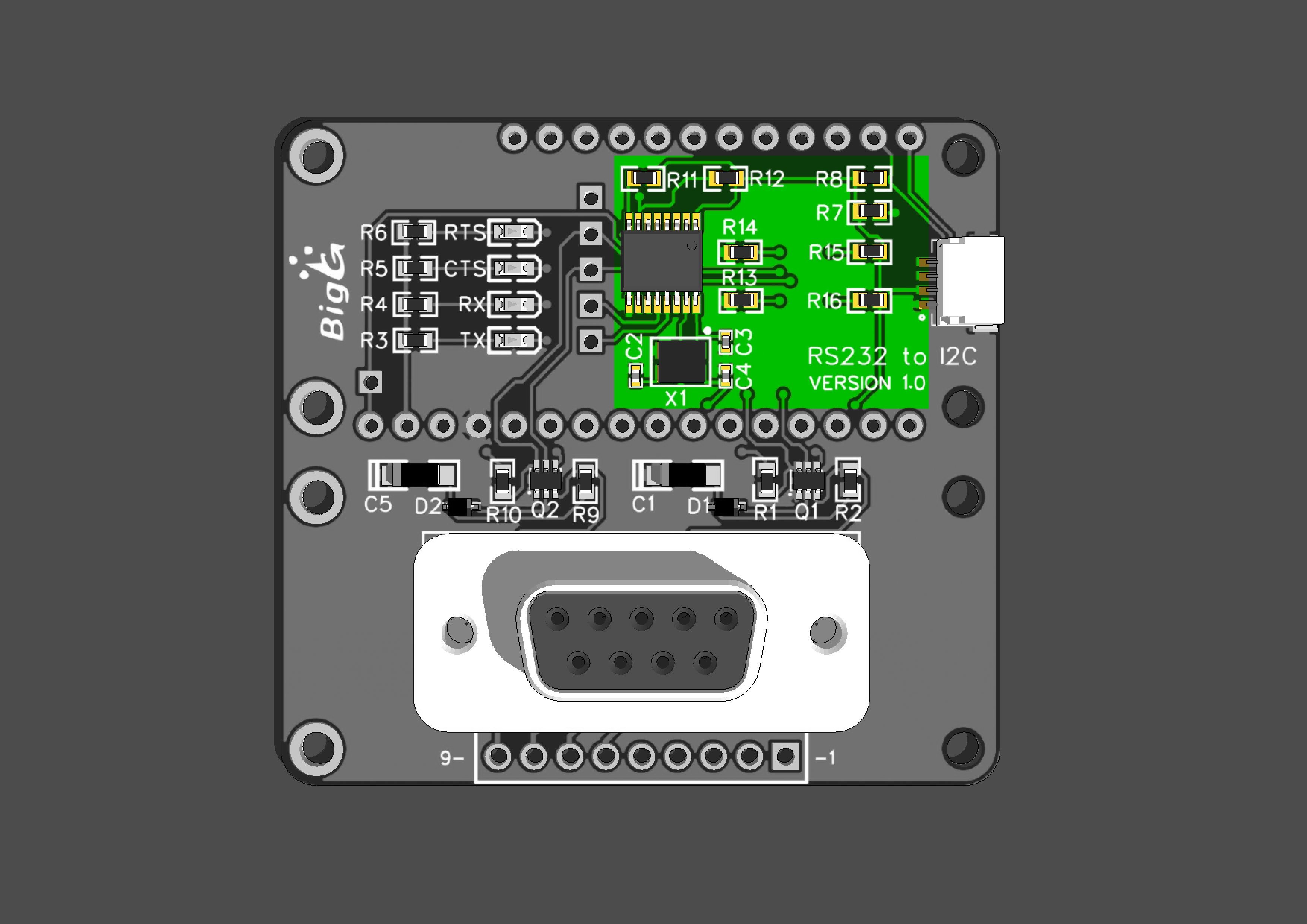
The I2C conversion circuit is based on the NXP SC16IS741 chip. I've attached the product datasheet for reference. This is handles a single UART channel with I2C-bus/SPI interface, 64 bytes of transmit and receive FIFOs.
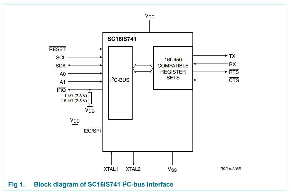
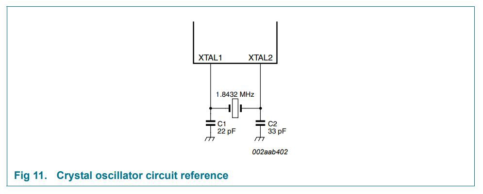
The SC16IS741 chip relies on an external 1.8432MHz crystal oscillator. This choice of oscillator defines the available baud rate and associated accuracy.
The only pins that are hard wired to the Feather pins are the I2C bus SCL and SDA lines.
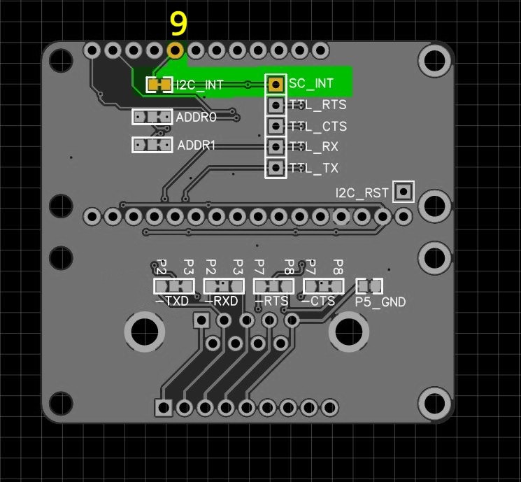
The I2C SC16IS741 chip also has an option for an Interrupt (open-drain, active LOW). The interrupt output is hardwired to pin 9 but this can be disabled (via solder joint) and then you can use the SC_INT option instead.
Four I2C slave address options are provided here, via ADDR0 & ADDR1.
I routed both address pins to ground (VSS) which sets the SC16IS741's I2C slave address to 0x9A.
Of course, this default could readily be changed to have both address pins pulled up to VCC, which would set the slave address to 0x90.
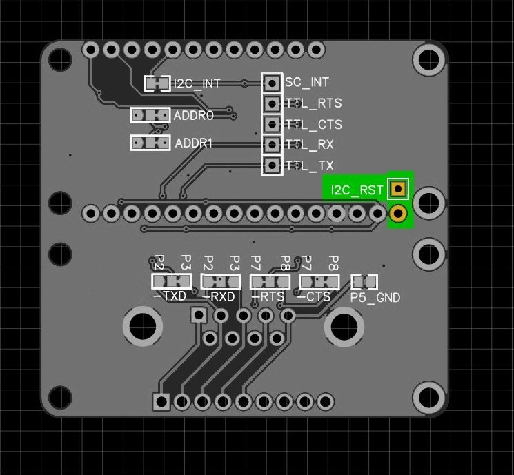
I also routed the SC16IS741's RESET pin to the reset pin on the feather, but I provide an exposed trace to disable this and allow the user to manually control the reset function.
I have also added a STEMMA QT (JST SH) connection for added convenience to allow for sensor connection etc. And that is basically it.
As footnote, I just wish to state that this is Version 1.0 of the board design and has yet to be fabricated.
 Kent
Kent
 Alastair Young
 SimonXi
 HappyFox