0%
0%
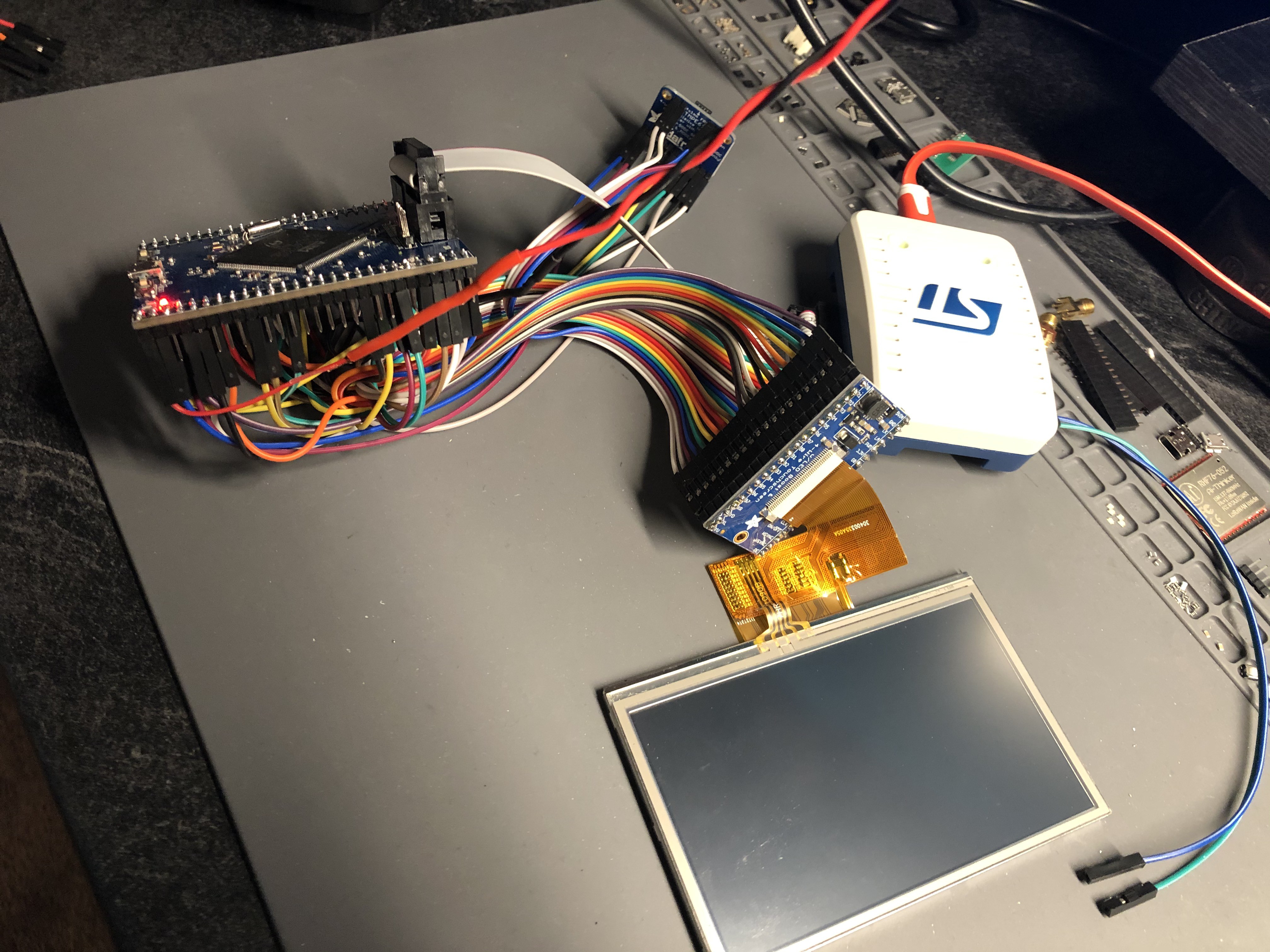
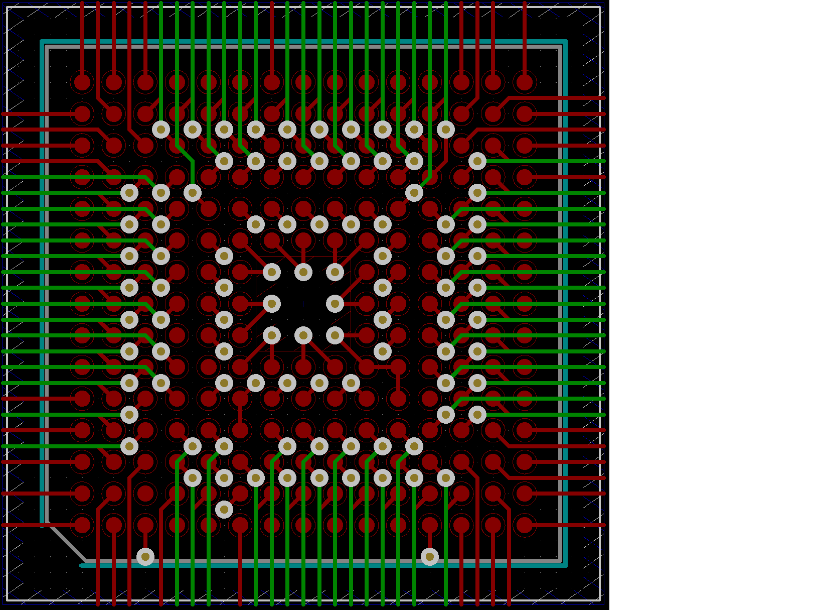
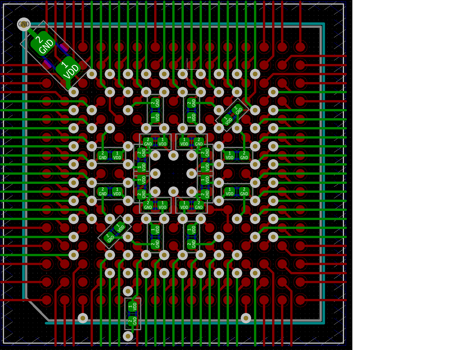
Open STM32 Minimal Display Board
An open sourced STM32 bare bones display driver board
 Andy
AndyBecome a Hackaday.io member
Already have an account? Log in.
Just one more thing
To make the experience fit your profile, pick a username and tell us what interests you.
Pick an awesome username
hackaday.io/
Your profile's URL: hackaday.io/username. Max 25 alphanumeric characters.
Pick a few interests
Projects that share your interests
People that share your interests


 Casual Cyborg
 Jackson Keating
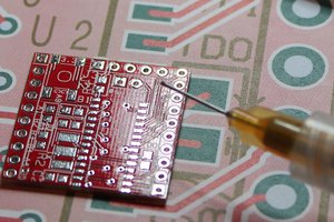
Fascinating read, any further updates? I'm attempting to do the same thing; build a touchgfx capable board that can be hand soldered. I've got as far as developing a system using the STM32F769DISCO and now want to build a custom version. Just ordered the stm32f767 Dev board before I stumbled on to your project. I'll take a look into the Adafruit modules as that'll save me some time designing a separate PCB for now.