 Andy
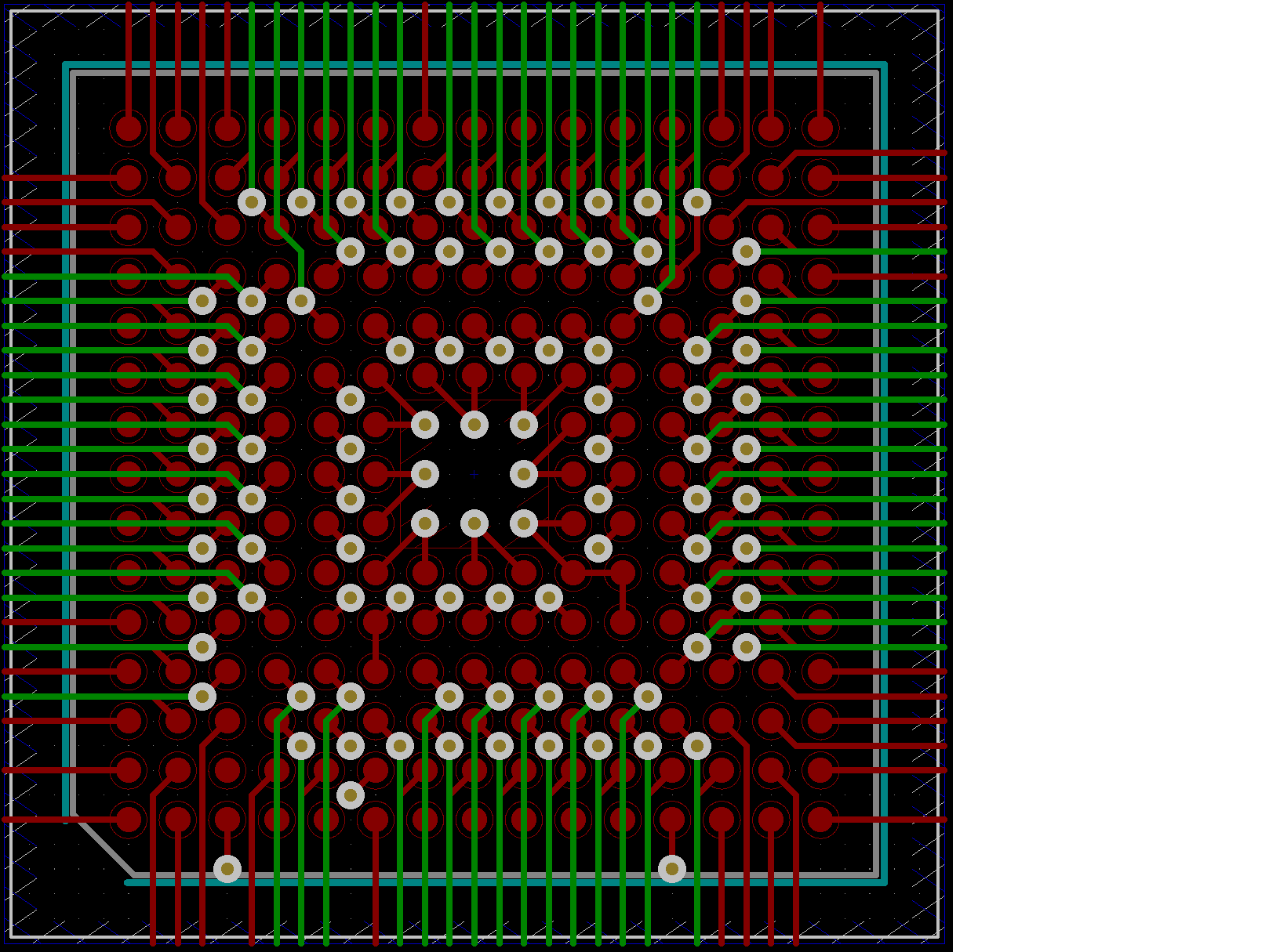
AndySo, as mentioned earlier, using standard design rules for the PCB you can completely fan out ST's TFBGA 216 package. Those standard PCB design rules are 4mil trace and space and .45mm via (17.7 mil). This is JLCPCB's multi-layer board minimums. OSHPark is a little more restrictive and has 5mil trace and space with 18 mil via. I didn't run the BGA fan out against the OSHPark rules, so someone would have to check that if they want. I tend to use JLCPCB most of the time anyway. Here's a picture of the complete fan out:
ST did a pretty good job of placing the power and ground pins so that you could use this package on a 4 layer board. Of course, it's no good if you can't get the decoupling caps in there. So here's a look at the fan out with decoupling caps:
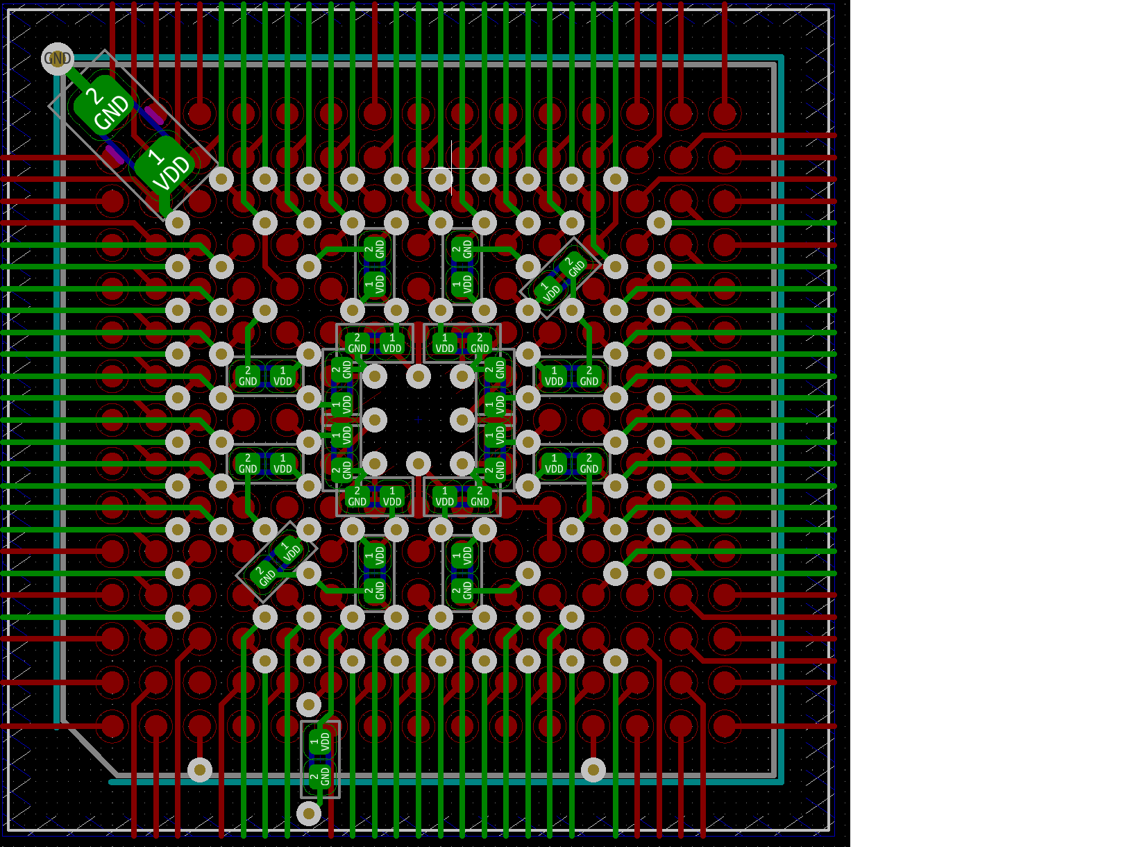
That's the required number according to the data sheet. This doesn't include a couple of power pins like Vdda and Vref as you'll usually have ferrites and other filtering on those. The smaller caps are 0402 which, for me, is about the limit of hand soldering. The larger tank cap up in the corner is 0805.
That's 100% fan out, does a pretty good job of not chopping up the GND and VDD power planes.
However, once you start to try to route out an SDRAM chip with a standard pinout, the idea of using a BGA starts to fall apart.
I was planning on using a MT48LC4M32B Micron SDRAM chip as it the same one used on the ST dev boards. You can also fan out the VFBGA-90 package that comes in, but it's pretty tough to fully connect the two with only four layers. I'm choosing to use a 32-bit data path and 13-bit address path which ends up being 57 total connections between the two devices.
While I'm sure it's possible to do on four layers with careful routing and tons of time, I have a feeling it would be almost impossible to route out any of the other pins. And while I would be OK with losing a few I/O, I think it would end up taking out the possibility of using most of the other peripherals.
You could go to 6 layers and JLC still offers hobbyist friendly 6 layer fabrication, but its pricey. At the time of this writing they will do 100mm by 100mm 6-layer for 87USD (qty. 10) at a build time of about a week. That's actually really amazing when you think about it, but I was hoping for something cheaper.
All that being said, I'm going to scrap the idea of using the BGA packages. However, once you start to look into the alternatives some interesting ideas start to evolve...
Til next time
Discussions
Become a Hackaday.io Member
Create an account to leave a comment. Already have an account? Log In.
I’ve been wrestling with the STM32WLE5 in the 73 pin 0.5mm BGA on Kicad and you’ve done much better than me! Could you share your DRC rules and BGA pad sizes please, as I cannot get the internal vias like yours even though I have set the same 0.45mm jlcpcb sizes.
Thanks!
Are you sure? yes | no