 MS-BOSS
I promised this log for several times and now it is finally here. Let's start with how a rising edge looks.
Risetime
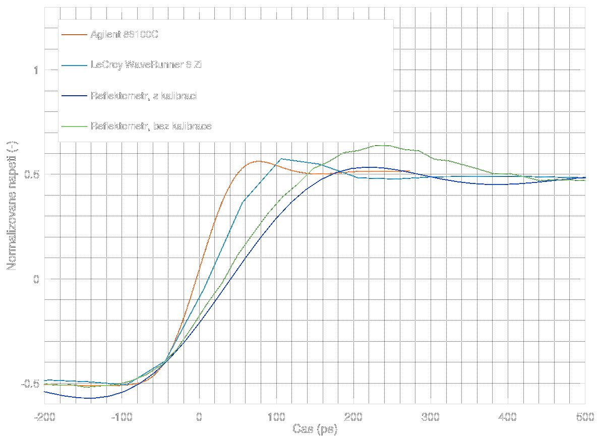
The orange and light blue ones were measured using commercial devices, the Agilent 86100C and LeCroy WaveRunner (this one was already mentioned last time). As you can see, the Agilent has the highest risetime (its bandwidth is about 26 GHz), about 89 ps which corresponds to the true waveform of the CML buffer pulse generator. Then the LeCroy, which cannot cope with the risetime and even shows low sample rate (about 25 GSa/s). The green trace is the reflectometer without SOL calibration and noise reduction, the risetimeis about 220 ps. The calibrated reflectometer output with noise reduction is slightly slower and shows pre-echo on the edge due to restricted spectrum.
Bandwidth and SNR
The SNR is a semi-measured parameter since it uses measured noise and estimated Gaussian pulse. The resulting SNR touches 0 dB at 2.5 GHz and goes under 0 dB near 3 GHz. So, the estimated useful frequency range is about 2-2.5 GHz.
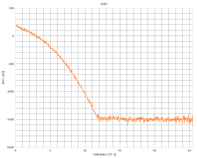
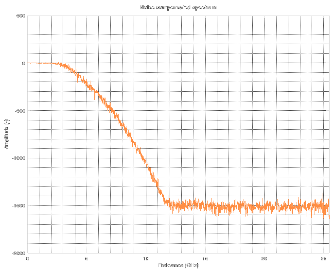
The resulting Wiener filter is nearly equal to 0 dB until 2-2.5 GHz and then sharply cuts off the spectrum. The resulting spectrum of the reflectometer after SOL calibration and noise reduction looks like this. The calibration seems valid until 2 GHz, then noise starts to emerge and the filter starts cutting it.
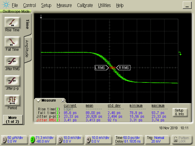
Pulse generator parameters
Here you can see the falling edge of the pulse generator, its fall time and its jitter. The jitter is measured between one unused output of the Si5351 and the pulse generator output. So, it doesn't tell us anything about jitter between the two VCOs of the 5351. I couldn't come up with any method of measurement of jitter between the two asynchronous outputs.
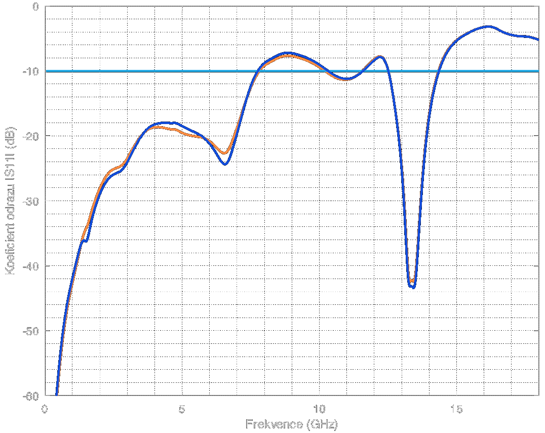
![]() Test port impedance
Test port impedance
 Test port impedance
The input impedance looks quite good until 3.5 GHz. Since the working frequencies of the reflectometer are less than 3 GHz, the input match could be called as "better than -25 dB" which is extremely good. On gigher frequencies, you can see it gets really bad, mostly because of the bad footprint of the SMA connector. Also, the connector is the cheapest Chinese SMA connector ,which doesn't help much with the results. However, in the useable band, the match is quite good. Also, as you may have seen in the log about SOL calibration, the reflection is small enough to be completely suppressed by the calibration.
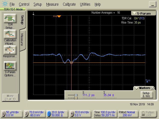
The TDR measurement of the port follows. The impedance drops to 35 Ohms for a while. The position of the impedance drop correlates with the SMA footprint on the PCB. The position was tested by using a sliding short and finding where the impedance drop lies. The sliding short was just the SMA torque wrench, no special piece of equipment. Another smaller impedance drop happens on the transition from the footprint to coplanar waveguide. One more impedance drop happens at the resistive splitter.
Noise reduction
The noise reduction comprises of averaging and Wiener filtering. The result of filtering is on the next graph. It helps, but is too time-consuming and doesn't get rid of all the noise.
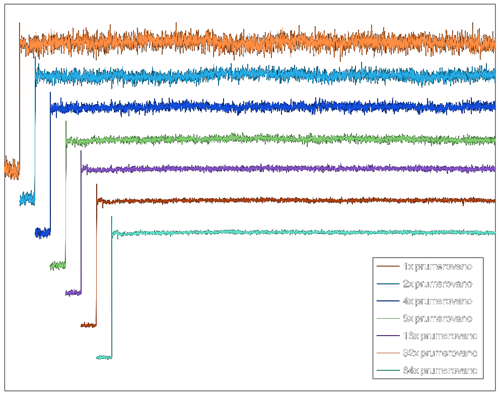
The Wiener filtering suppresses the noise left after averaging. The filter looks at the averaging used for LOAD calibration, NOISE calibration and averaging used for the measurement itself. The filtering works for both calibrated and uncalibrated data.
First, without noise reduction:
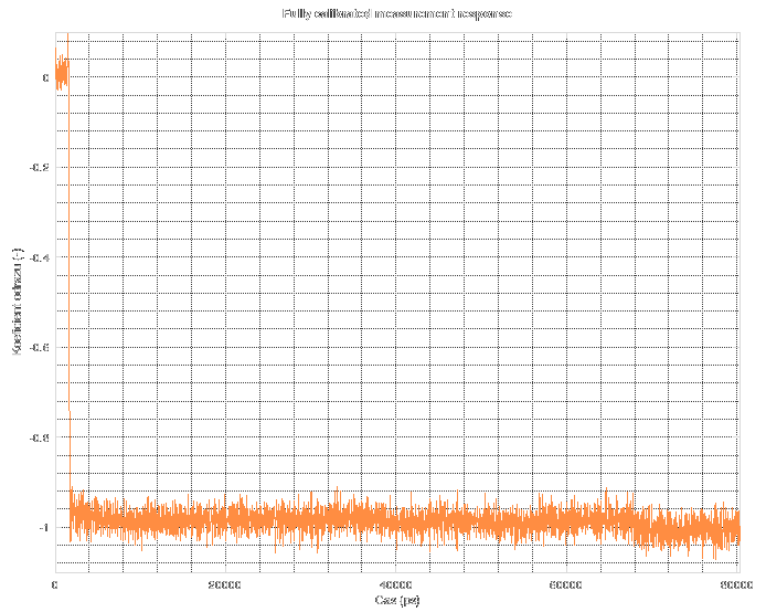
And with noise reduction:
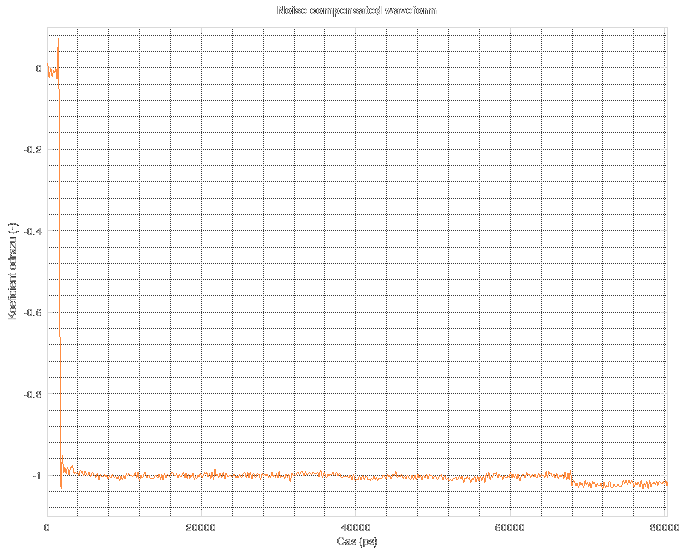
The step at 68 ns happens because the original data ends there and the rest is a prediction of future events made by the Fourier transform. But I do not know why the step happens, I would expect the data to continue with the same level, just filled with noise.
Conclusion
The reflectometer works and it is usable from DC up to about 2 GHz (maybe slightly over that with reduced SNR). The time resolution is 20 ps and can store 4096 points. It can be calibrated as one-port VNA which removes the side effects of mismatched impedance of its input. An adaptive noise suppression algorithm was implemented.
What now?
Now, I will move onto next project. Maybe it will be two-port TDR/TDT usable as a time-domain VNA (hae to figure out the 12/16 element calibration process). Maybe it will be a two-channel oscilloscope. It will be most probably based upon designs of "loxodes", Darwin Sabanovic and Ted Yapo. All of these designs are practically the same, even with the same impractical bits here and there.
I already have a few ideas how to make the oscilloscope...
 Now, I think I have already exhausted all the interesting themes of this project, so I will probably stop writing logs about this project and we could move on to discussion in comments section.
Discussions
Become a Hackaday.io Member
Create an account to leave a comment. Already have an account? Log In.