 Bud Bennett
Twice in the last couple of years I have needed a probe to diagnose problems with a non-isolated power supply that connected directly with the 125VAC mains voltage here in the USA. I have been able to work around it by using less than satisfying methods. My cheap oscilloscope (a Rigol DS1102E) is good enough for most of my purposes, but the math function to subtract Channel 1 from Channel 2 really sucks. And even though it is a cheap scope, I'd rather not have to buy a new (more expensive) scope because I connected the scope ground incorrectly.
Needing a tool on a yearly basis hardly qualifies as necessary, but I had some down time waiting for components and PCBs for another project and began to consider this as an interesting project.
There are now three versions of this probe. My original version that is powered by a 5VDC adapter, Paul's new version is powered by any adapter in the range of 7-12VDC, and a 1X version -- see Christoph's Project. Paul made some changes to increase the creep distance between the input pins since he needs to use it with 240VAC mains. You can find the Gerber files, BOM and schematics for Paul's version on his Github Page. Christoph's 1X probe uses my design, but changes the attenuator to achieve higher differential gain at the expense of lower common mode range.
I'd been following Paul Versteeg's progress to make a differential probe on his blog. I recommend that you read it -- he covers most of the basics and has some good references of other approaches to make this kind of probe. Paul has done more thorough testing as well (his equipment is better than mine.) He also spent a lot more effort explaining how to assemble the probe and calibrate it. There are also several persons within Hackaday that have completed projects successfully, or are still ongoing.
The Specifications:
- Input impedance: 20MegΩ// 1.25pF - differential, 10MegΩ//2.5pF each terminal to GND.
- Differential Gain = 1/10 V/V. Any lower than this and the DS1102E could not resolve a 1V signal with any clarity. (Many of the cheaper differential probes are switchable between 50X and 500X attenuation. This would be good if the signals in which you are interested are very large, but that's not the case so far with my needs. The better probes ($400 and up) provide 10X/100X attenuation.
- Common Mode Range > ±340V (240VAC produces a sine wave 679V peak-peak)
- CMRR >90dB @ DC, ~60dB @ 1MHz
- Differential Voltage Range > ±24V for 240VAC common-mode, ±24V for 0V common-mode (Paul's version increases both ranges to ±25V)
- Bandwidth ≥ 100MHz (Dependent upon signal amplitude) This will be a stretch for my current skill set.
- DC offset < 20mV
- Noise: 2.2mVrms at output.
- Cost: ~ $50
The completed probe:
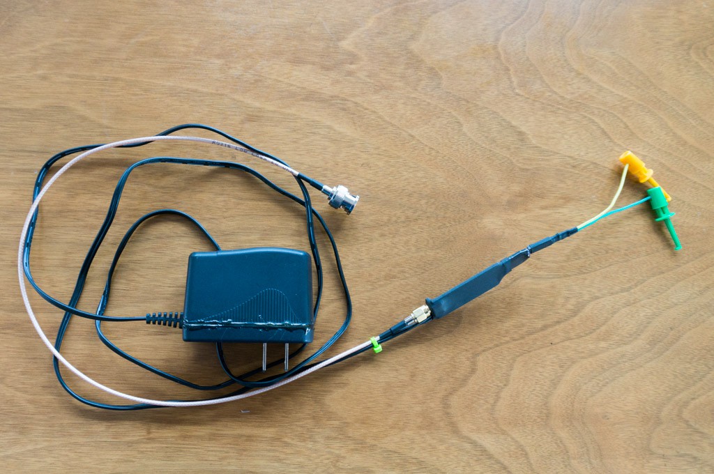
The above photo is my completed probe. You will need a 5VDC adapter to power Bud's probe or a 7-12VDC adapter to power Paul's probe, and a SMA to BNC pigtail to connect the probe to the scope. You should also consider making a few leads for various situations. The leads use a Dupont 0.1" (2.54mm) 2-pin female connector to attach to the probe. The green tie-wrap provides a bit of strain relief for the power supply leads into the probe.
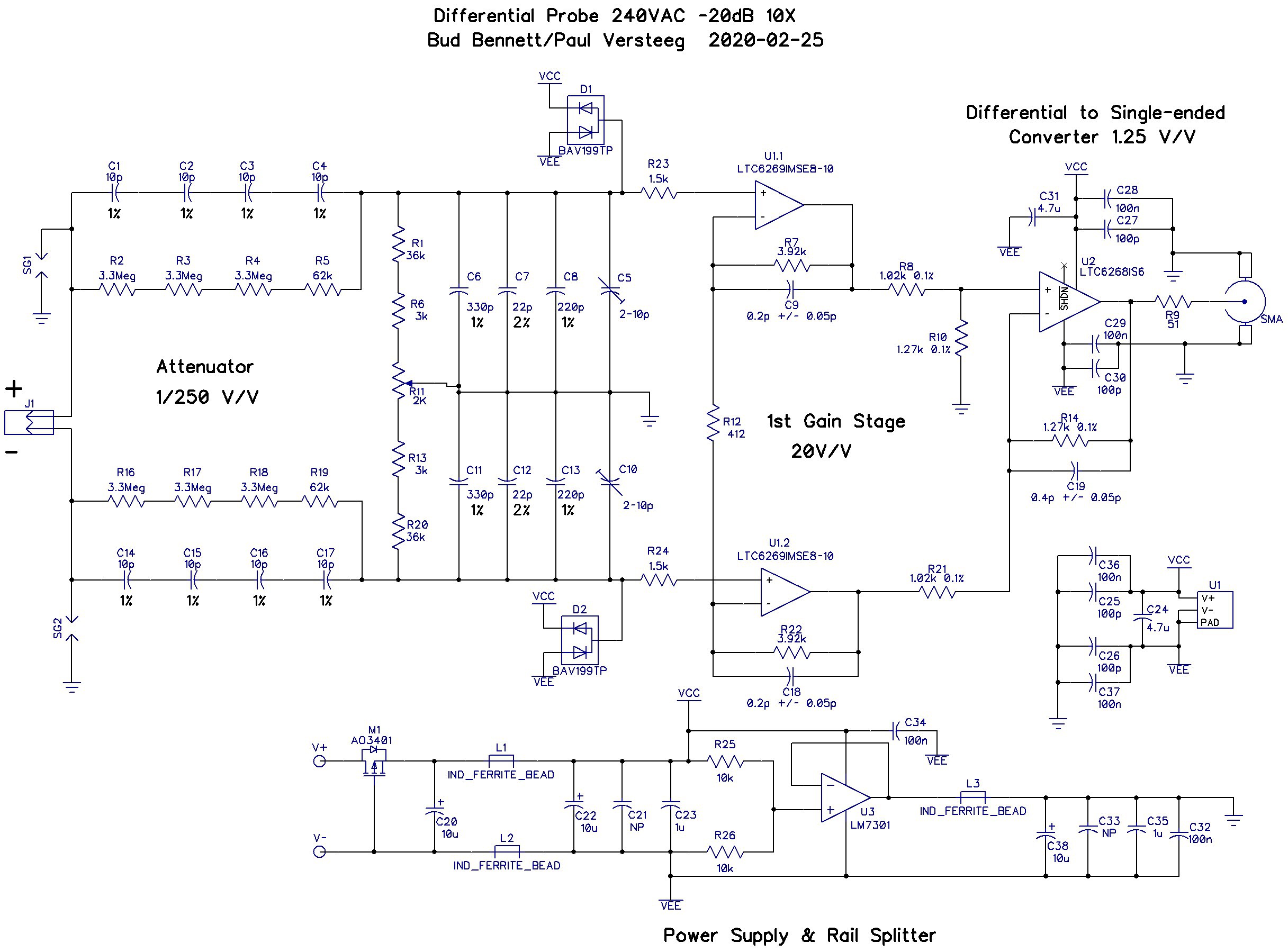
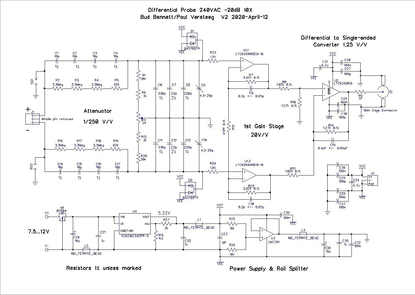
The Schematics:
There are now two versions of this probe.
The 5V adapter version (Bud's):
The 7-12V adapter version (Paul's):
[Edit 2020-01-30: Improved the differential range with a 240VAC input to ±24V with small changes to component values. No change to the PCB layout.]
[Edit 2020-02-05: More conservative design for the first gain stage stability. Replaced BAV99 diodes with BAV199.]
[Edit 2020-02-13: Increased R23 and R24 to 1.5k from 510Ω to reduce ringing with fast input step.]
[Edit 2020-02-25: Changed C6-C8 and C11-C13 to match lower capacitance of the 10pF input capacitors. Your mileage may vary.]
[Edit 2020-05-10: Changed C19 to 0.4pF±0.05pF to match Paul's schematic. He found the bandwidth not quite 100MHz so reducing this capacitor boosts it by 20%.}
The input attenuator is 250X. The series R and C network is necessary to avoid exceeding the voltage rating on any of the components when subjected to high voltages. The resistors attenuate the low frequencies and the capacitors attenuate the higher frequencies. Both networks require a trim to reduce common mode rejection at low frequency, and gain and common mode rejection at high frequencies. 1 percent tolerance components help to keep the trim ranges small. Spark gaps, SG1 and SG2, and clamp diodes, D1 and D2, limit damage from ESD or inadvertently exceeding input voltage specifications.
The first gain stage has a differential gain of 20 V/V and a common mode gain equal to unity. This stage recovers some of the attenuation that was necessary to provide a relatively large common mode range. These amplifiers need a gain-bandwidth (GBW) greater than 2GHz in order to meet the 100MHz system bandwidth requirement.
The second stage is a differential to single-ended converter with a gain of 1.25 V/V. Its GBW should be around 200MHz. R9 matches the 50Ω impedance of the expected coax cable to the scope, even though the scope input is 1MegΩ//15pF. R9 should absorb reflections due to the unterminated coax transmission line -- it's not perfect, but better than nothing.
The circuit that occupies the bottom develops the power supplies. The input current requirement is 50mA provided by a simple DC wall adapter. Ferrite beads and capacitors should clean it up nicely. U3 splits the ±supply rails to generate a GND rail halfway between VCC and VEE.
Initial Simulation Results:
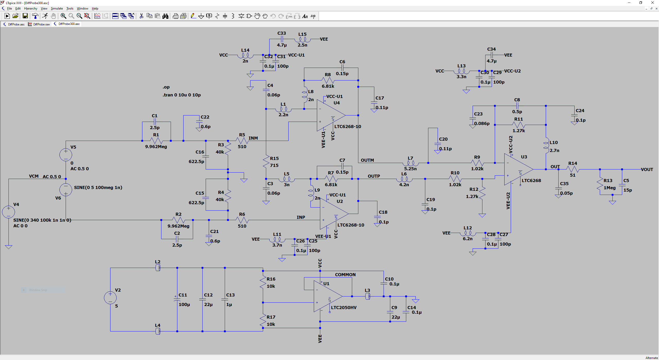
Here's the LTspice schematic of the basic circuit without any PCB parasitic back-annotation (I've added this file to the files section of this project):
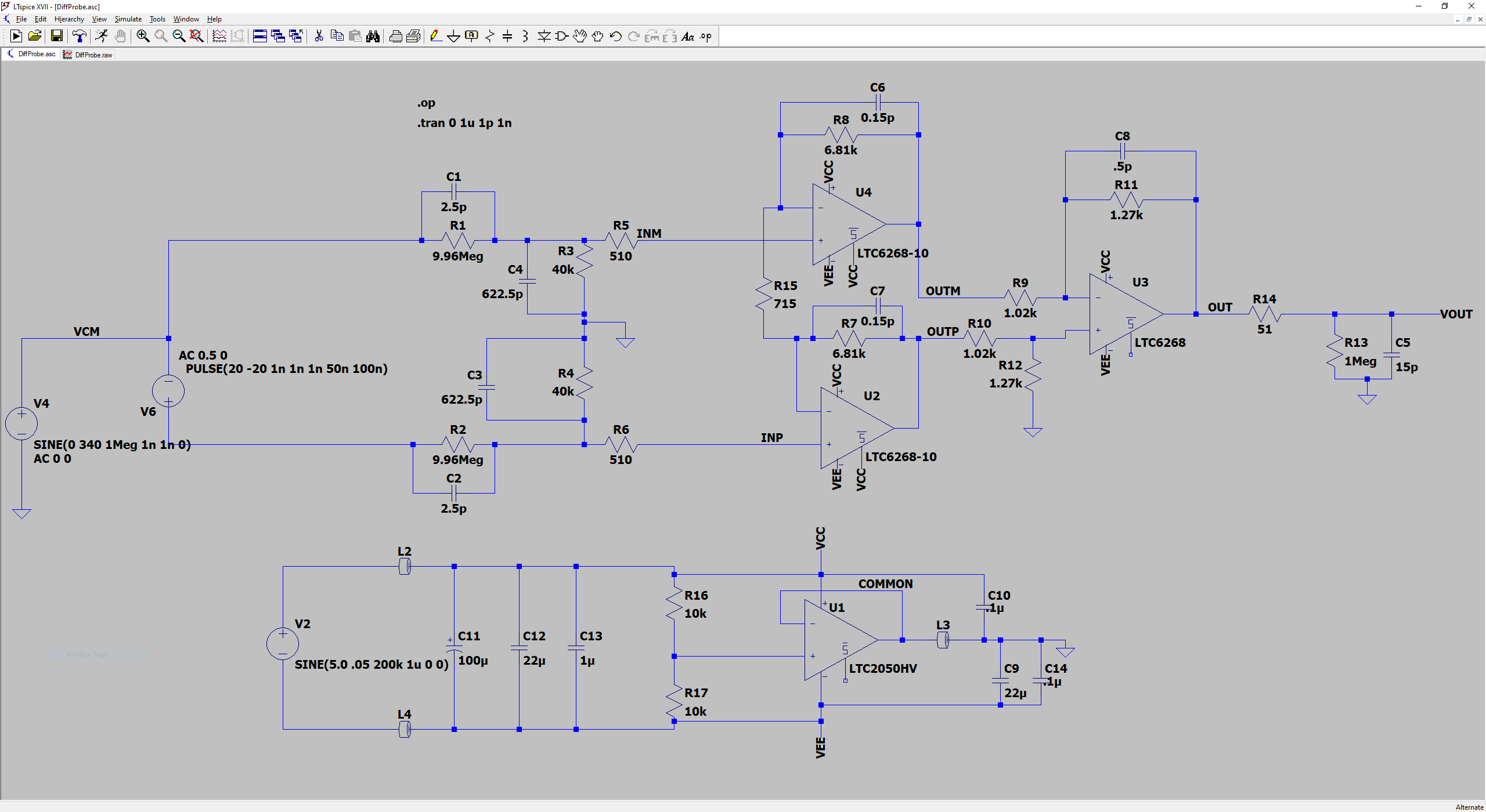
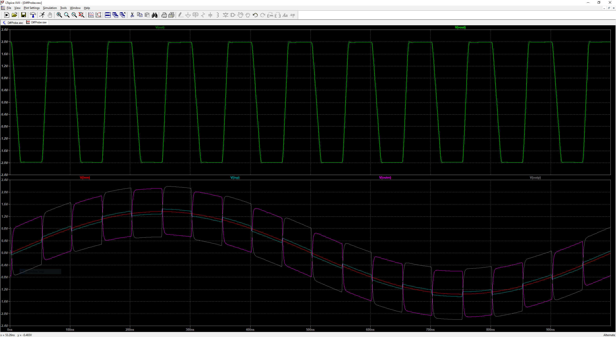
The simulation results are promising. This plot shows the output of the probe (top trace) for a 20V/10MHz square wave input riding on a 340V-peak/1MHz common mode voltage. The slew rate limitations of the output stage are clearly visible with this large signal input.
Design Details:
There is a lot of material to digest prior to embarking on high-speed PCB design. I collected the following tutorial papers:
- AN-148: Does Your OPAMP Oscillate?. By Barry Harvey. Specifically references the LTC6268 and LTC6268-10.
- A Practical Guide to High Speed Printed Circuit Board layout. By John Ardizzoni.
- High Speed Analog Design and Application Seminar. By Texas Instruments.
- AN-1368: Ferrite Bead Demystified. By Jefferson Eco and Aldrick Limjoco.
- The Secret World of Oscilloscope Probes. By Doug Ford. I should have started here.
- High Speed Amplifier Techniques. By Jim Williams. Dated, but full of good examples.
Some of the material is contradictory or anecdotal. You must decide for yourself if it applies to your situation.
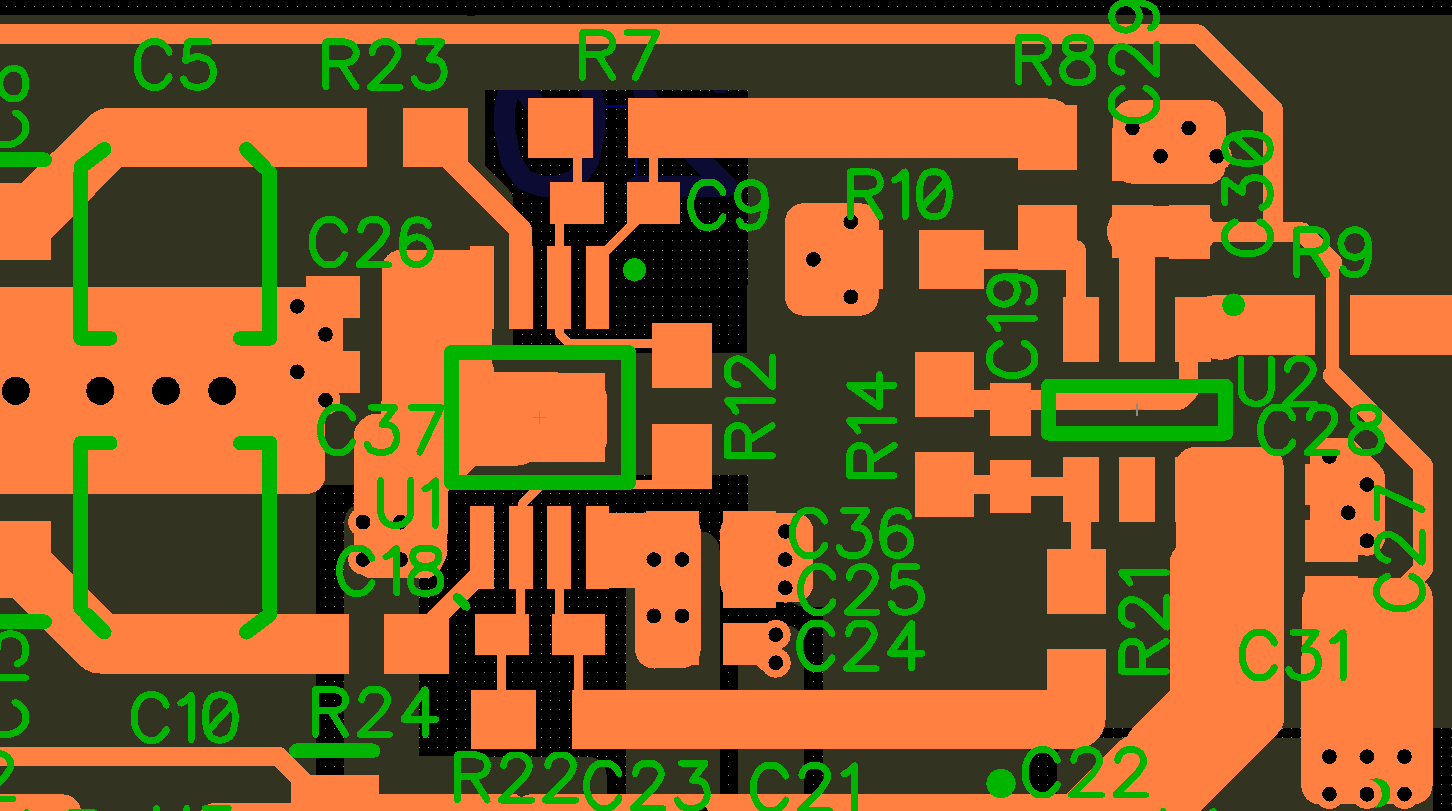
The Layout:
The PCB layout is closely coupled with the schematic. These three views of the PCB will be referenced frequently in the following explanation of the design process.
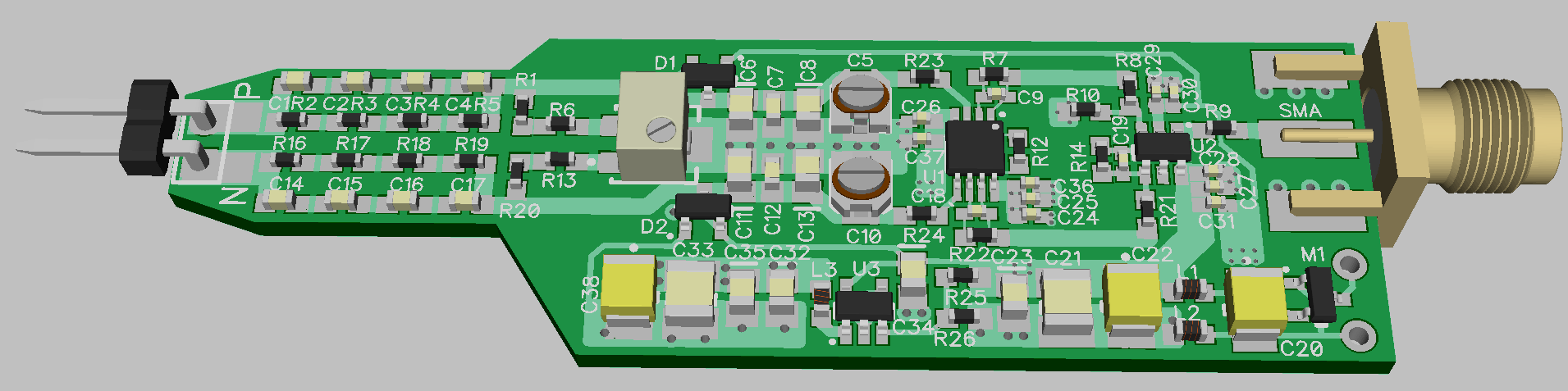
A view of the populated PCB.
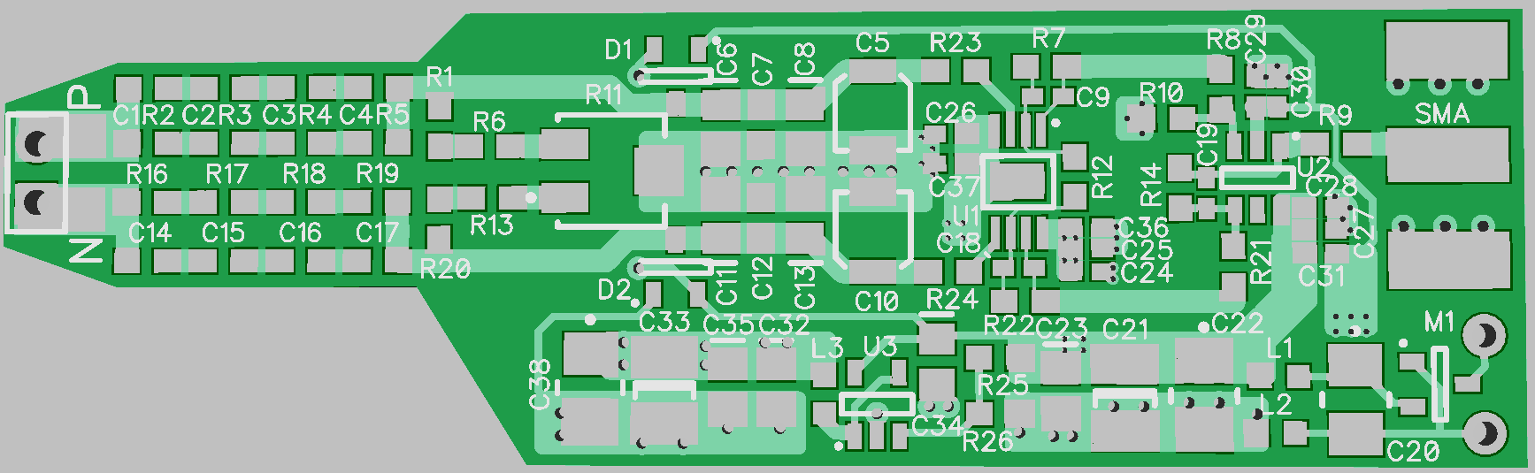
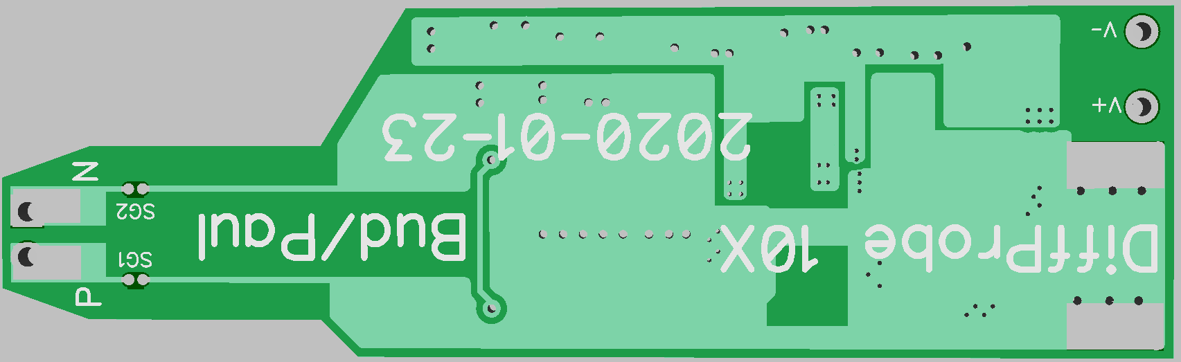
The unpopulated PCB top and bottom side, showing more clearly the connectivity, traces and ground and power planes. It is more of a challenge using 2-layer boards, but that is my only choice, given the limits of the free version of the Diptrace software. The overall dimensions are roughly 0.75" x 2.5" (inches are still the default unit of measurement for PCB layouts -- go figure.) The probe "tip" is about 0.25" to help when probing inside tight spaces.
The spacing between the positive and negative inputs is 0.8mm. The minimum spacing to withstand 250Vrms between two bare copper traces is either 0.56mm or 1.5mm, according to this document and its links. I might have to cut a slot between the two conductors to improve the "clearance or creepage", or widen the spacing if there is a subsequent PCB revision.
The Attenuator:
The attenuator includes all of the components from the input terminals to the two protection diodes, D1 and D2. It is simply a resistor divider at low frequencies, and a capacitor divider at high frequencies. The resistors and capacitors are 0603 size, 1% tolerance, to make the layout simpler. In addition, the capacitors are NP0 type with a rating of 200V. The 0603 resistors are typically rated for 350V.
NP0 capacitors don't exhibit any variation in capacitance vs. applied voltage (unlike other dielectric types) -- see this website. The NP0 tag means negative-positive-zero, but can have a temperature sensitivity as high as ±30ppm/°C. That's still a lot better than X7R or X5R, or heaven forbid Y5Anything.
The DC gain is nominally 40k/(9.962Meg + 40K) = 1/250.05 V/V. The 3224j potentiometer is a 10% tolerance, 11 turn, which could add a 0.25% error. (Alternatively, a 3314j pot with 20% tolerance and only 240° turn could be used.)
The AC gain is nominally 2.5pF/(622.5pF+2.5pF) = 1/250. The trimmers are 1/2 turn 2-10pF (-0%, +100%). If the 15pF and 300pF capacitors are at the end of the tolerance range they could vary ±4.25pF (0.71%), with the diodes contributing another 1.5pF and the PCB trace another 0.6pF. If the trimmer cap can't go low enough the 15pF capacitors, C7 and C12, could be 12pF or 10pF to recover some trim range.
The attenuator layout is absolutely symmetrical between the positive and negative signal paths. There is no ground plane under the front portion of the attenuator. This is to keep parasitic capacitance to a minimum. I ran a thin GND trace between the resistors and capacitors to provide a return path for the spark gaps. This trace is equidistant and symmetrical between the components so I'm hoping it has negligible impact. The ground plane under C5-C8 and C10-13 is OK because the total capacitance is more than 600pF, but the ground plane under R1, R6, R13, R20 is removed to minimize parasitic capacitance.
The diodes, D1 and D2, protect the inputs of U1 from overvoltage/overcurrent. The LTC6269-10 specifies an absolute maximum voltage of VCC+0.2V or VEE-0.2V, with a max input current of ±1mA, at the input terminals. D1 and D2 will clamp the inputs to VEE-0.7V and VCC+0.7V with R23 and R24 limiting the current into the pins to less than 1mA. At high temperatures D1-D2 could leak currents into the inputs and cause offset errors, but I'm betting that the board temperature won't get much above room temperature (25°C ±5°C), since total power dissipation is only 250mW. Typical leakage current per diode is about 400pA @ 25°C (max leakage = 5nA).
First Gain Stage:
The core of the first gain stage has only six components, but it requires the most care to obtain good results. I found the LTC6269-10 through a paper titled, "LTC6268-10 Oscilloscope Differential Probe." The circuit was AC-coupled and had a very small common-mode range, but the amplifier was pretty amazing:
- 4GHz GBW
- ±0.7mV input offset voltage @ 25°C.
- ±31fA input bias current
- Rail-to-rail output
- Minimum closed-loop gain > 10 V/V.
- Slew rate +1500V/µs, -1000V/µs
- Supply range: 3.1V to 5.25V
- Common-mode input voltage range: -Vsupply to +Vsupply - 0.5V
This stage has a differential gain of 20V/V and a common-mode gain of unity. Originally, the gain was set at 10V/V, but it seemed marginally stable in simulation. The amplifier's bandwidth exceeds 100MHz with a gain of 20. The nominal differential DC gain is equal to 1 + (R7+R22)/R12 = 20.029 V/V. C9 and C18, size 0402, compensate the phase shift associated with the input capacitance of the opamp's minus input. There is no worry about input bias current causing offsets because the currents are so low (even over temperature.)
The value and tolerance of C9 and C18 determine the values of R7, R22 and R12. It is nearly impossible to get a tight tolerance 0.15pF capacitor, unless you are willing to order 10k of them. The best I could find was a 0.2pF ± 0.05pF in low quantities. R7 and R22, in order to meet the 100MHz bandwidth requirement, with a maximum value of 0.25pF for C9 or C18, were limited to a maximum value of 4.1kΩ. Therefore I selected 3.92kΩ for R7 & R22, and 412Ω for R12 to approach a gain of 20 V/V. When C9 or C18 are at the low end of the tolerance the amplifier is still stable, with some margin (it doesn't break into oscillation until C9 or C18 drop below 0.09pF).
I wanted relatively high resistor values for the feedback and load -- the smaller currents will allow the output stage to get closer to the supply rails and yield more input voltage range before clipping. Also, lower currents in the output stage may prevent the output stage from oscillating by itself with parasitic LC elements. With the GND rail set at (VCC - VEE)/2 = 2.5V above VEE, the output voltage can typically swing within 25mV of VEE and 40mV of VCC, while the inputs can swing between VEE -0.1V and VCC - 0.5V. A 240VAC sine wave will apply 1.36V-peak common-mode voltage to the inputs, and outputs, of the amplifier. A differential input voltage can add up to +(VCC - 2.5 - 1.36 - 0.04)/10 * 250 = +27.5V or -(2.5 - 1.36 - 0.025)/10 * 250 = -27.8V before the outputs saturate.
It is worth mentioning that the inputs don't clip until the added differential voltages exceed ±60V with 240VAC common-mode applied.
First Gain Stage Layout:
This amplifier is extremely sensitive to parasitic capacitance and inductance in the PCB traces. Therefore I removed the ground plane under the sensitive inputs/outputs and minimized the interconnect lengths. All of the components are located on the top side -- eliminating inductive vias.
R23 and R24 are moved close to the positive inputs of the amp. I'm not too worried about this, but it is better to have short leads on the more sensitive signals. C9 and C18 are as close as possible and a small 0402 package. R7 and R22 are also very close and use minimum PCB trace widths. The problem is R12 -- the ground plane can't be removed under it so it will have a larger parasitic capacitance and the leads are long and skinny, which creates inductance -- but I could see no better option. The amplifier outputs are wide, to reduce inductance, and as short as possible to minimize capacitance over the ground plane.
All of the bypass capacitors are 0402 -- to increase the self-resonance frequency of the cap. There is a 100nF in parallel with a 100pF connected to from each supply to GND, and another 4.7µF connected between VCC and VEE. I found this webpage which has an excellent graphic showing self-resonance frequency vs. capacitor value for 0402 and 0603 sizes. All of the bypass caps are connected with multiple small vias to GND or power leads that are short and fat. The supply currents are going to slosh back and forth across that short piece of ground plane; I'm hoping that it is a small enough inductance to not create a problem.
Common Mode to Single-ended Converter:
There is nothing special about this amplifier. It simply converts the differential output of the first stage to a single-ended signal to send to the scope. Closed-loop gain is 1.27/1.02 = 1.2451. I decided to go with 0.1% tolerance for the resistors. Paying $0.30 per resistor is not exorbitant, and I get ±25ppm TCR to go with it. I learned that the trim pot can remove the common mode term at near DC, but at higher frequencies the capacitor mismatch and intrinsic CMRR of the LTC6268 amplifier tend to dominate. Having tighter tolerances on the resistors yielded better results in simulation.
This amplifier must be stable at unity gain, so I selected the LTC6268 in a SOT23-6 package. It has a GBW of 500MHz which is good for a 100MHz unity gain bandwidth, but its slew rate is a bit low (400V/µs) for large signal swing integrity. It has rail-to-rail output swing and the common-mode input range exceeds the required 2.5V ±1.38V.
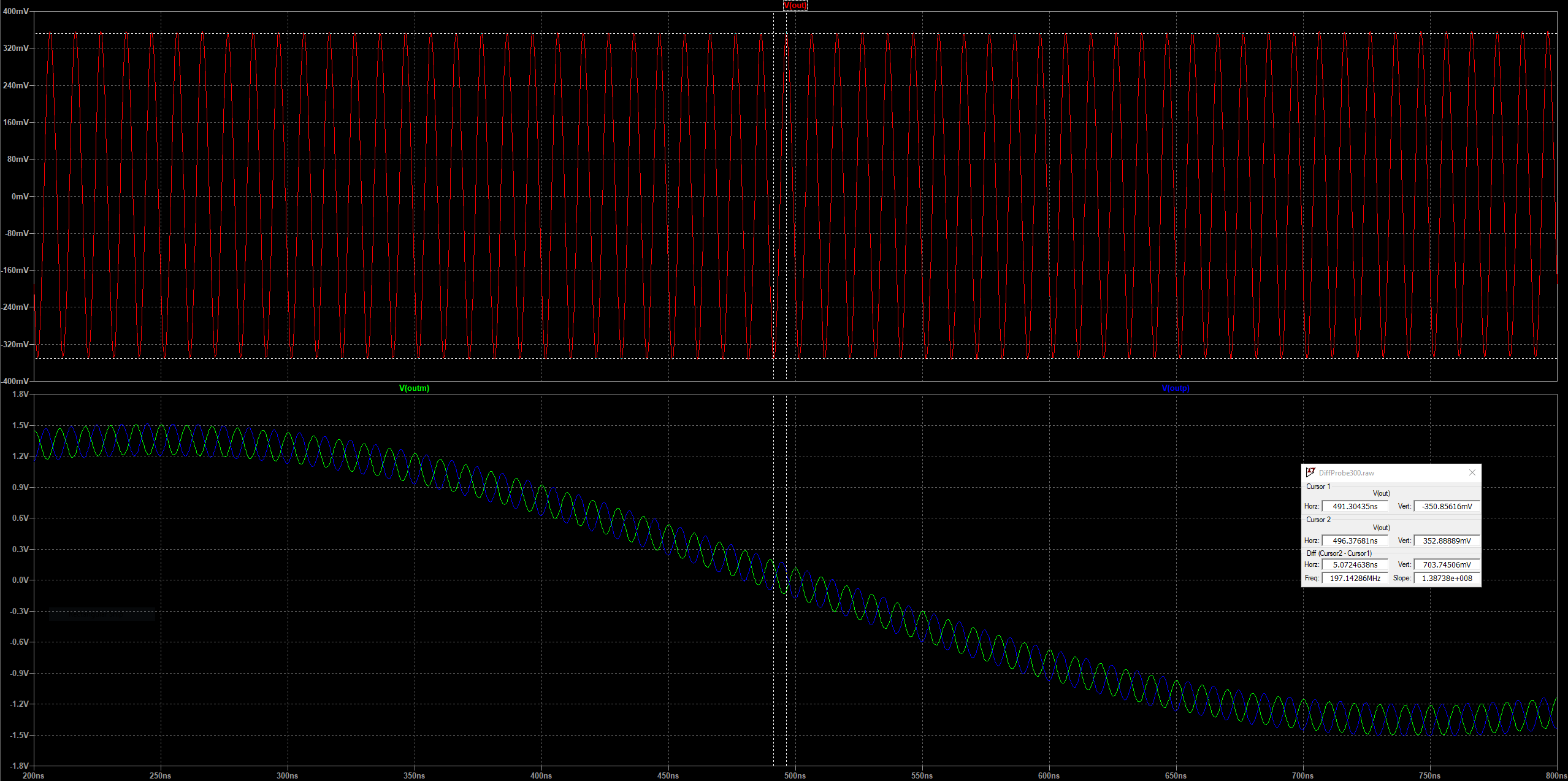
This simulation shows a 10Vp-p 100MHz sinusoidal input applied with a 340Vpeak 1MHz common-mode voltage. I would have expected the output voltage (top trace) to exhibit some amplitude suppression due to the slew rate of the output stage, but the amplitude is very close to the expected value at the -3dB bandwidth. A closer look reveals some distortion in the sine wave output near 0V, but the amplifier is able to recover, or catch up, as the sine wave slows at the positive and negative peaks. I doubt whether this would be visible on a scope display. Where the slew rate limits become clearer is when a large amplitude square wave is applied -- the duty cycle of the waveform is changed.
The layout is not as sensitive as the first gain stage. The ground plane is not broken, but all of the components are located as close as possible to the amplifier inputs to minimize parasitic capacitance. C19 sets the BW of the amplifier; it is 0402 and located next to the input pin.
The bypassing is the same as the first stage, but since there is an unbroken ground plane it should perform better. There is one funky trace from VEE to C29-C30. The added inductance doesn't cause any problems because the two bypass caps are very close to the opamp power pins and they have short leads/multiple vias to the ground plane.
Back-annotation:
After the layout arrangement was settled I measured the critical inductances and capacitances and back-annotated them into the LTspice simulation. In addition, I calculated approximate self-resonant frequencies for all of the bypass capacitors and added appropriate series inductance parameters to each bypass component. The results were underwhelming...no discernible differences from the original simulation results. The one change that I did make was to increase the feedback capacitor across the common-mode to single-ended converter from 0.4pF to 0.5pF, which compensates for the increased parasitic capacitance at the input pin.
Procedure to Compensate the Probe:
(For a better example of this process see Christoph's project log. Just be aware that he is compensating a 1X probe with lower CMRR and differential gain. Paul has a good description of this procedure in his blog, but you will have to scroll through a lot of stuff to get to it.)
I use a 30V power supply, a 2N7000 FET, a 5.6kΩ load resistor, and the scope's 3Vp-p 1kHz calibration signal. The FET and load resistor just translate the 3Vp-p calibration signal to a 30Vp-p square wave. Here are the steps:
- Connect both probe inputs to the 30V square wave and adjust the pot until the output is as flat as possible. There will be spikes from the uncompensated AC gain, but ignore them for now. This step cancels the DC common mode error.
- Reduce the power supply to 20V. Connect the positive input to the drain of the FET. Adjust the C5 to obtain a flat top/bottom of the square wave. This will match the positive signal path AC gain to the DC gain.
- Set the power supply to 30V. Connect both probe inputs to the 30V square wave and adjust C10 to eliminate the spikes seen in the waveform. This will match the AC gain between the positive and negative signal paths.
- You're done.