 Christoph
In the previous project log (https://hackaday.io/project/169390/log/194914-adding-a-more-sophisticated-scope-interface) I described a modified probe that allows to inject an offset current to adjust the probe. Some scopes have an interface that has additional connections to supply active probes, communicate with them and adjust them, and we're trying to make this probe compatible with that interface - at least the analog and supply part (communication will be added too, but closer to the scope connector).
While Bud was already pointing out some shortcomings of the modified schematic, namely gain error and lower CMRR, I had already ordered PCBs from aisler and assembled one once they arrived:
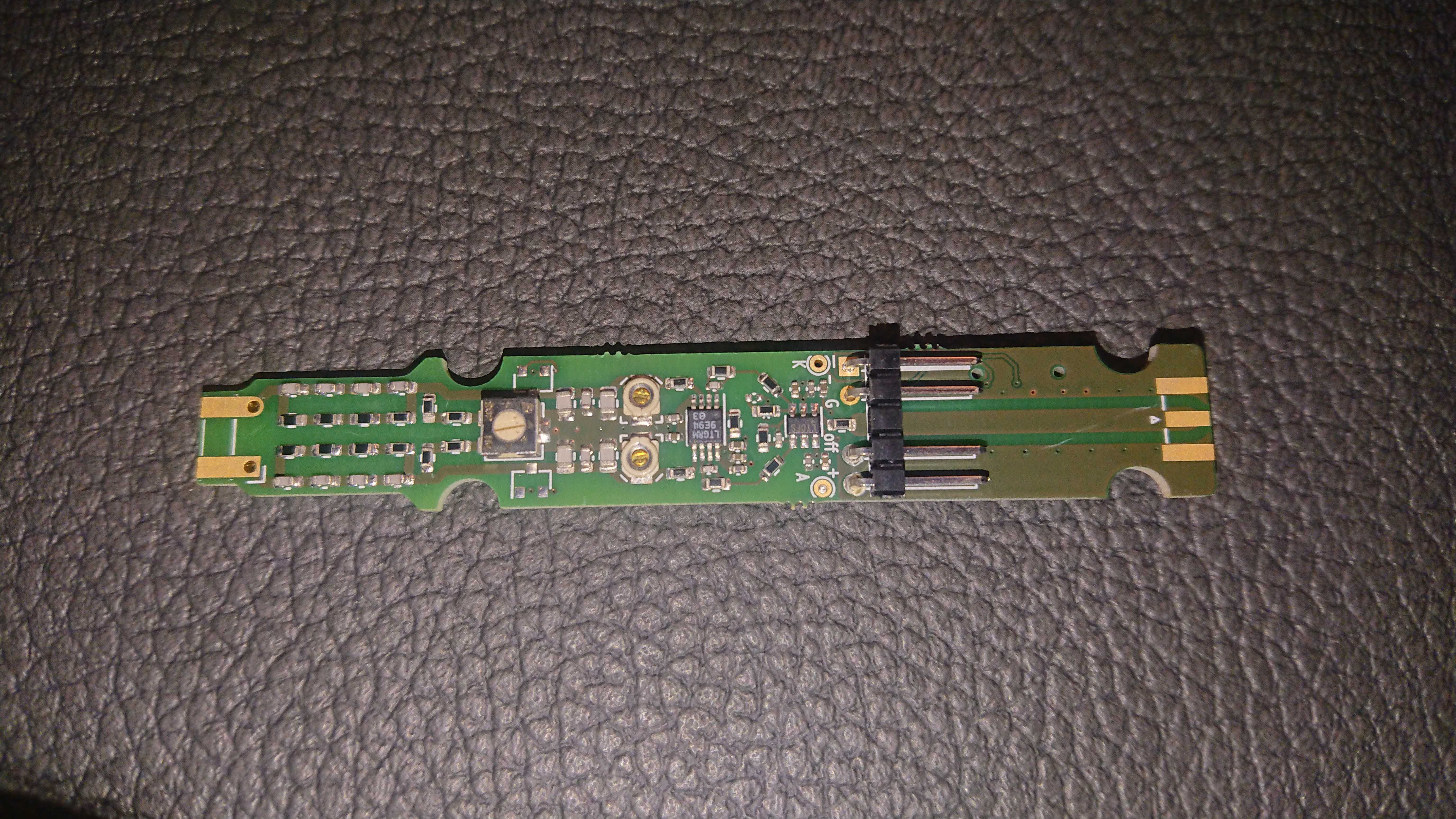
My plan was to assemble one even if it's not perfect, send it to another tinkerer who has the necessary equipment to test it thoroughly, and use his and Bud's feedback to adjust the next revision of the schematic, the layout and also the overall shape (for a 3D printed enclosure).
Note:
1) I didn't place protection diodes
2) The layout didn't contain spark gaps and their ground trace
3) an extra cap had to be added to the attenuator to compensate the probe. We'll get to that later.
Assembly was done with low temp solder (see here for the details about how I solder small/low temp stuff: https://hackaday.io/page/10792). However, swapping out caps was still tedious and time consuming because it's an iterative process.
Caps, Caps, Caps
I had previously built a probe as per Bud's original design and knew that the effective capacitance of C1...C4 is significantly lower than 2.5 pF (4x 10 pF caps in series). On his layout, the effective capacitance was around 2.31 pF (4x 9.25 pF in series), so C6...C8 had to be around 572 pF (+trim cap 2...10 pF) to get a 1:250 attenuator.
On my layout, the capacitance of C6...C8 had to be 593 pF (330 + 220 + 33 + 10 pF), which is significantly higher than on Bud's layout. We came to the conclusion that it's most probably the absence of the spark gaps and their ground trace that leads to this significant change in parasitic capacitance (obviously, this is something that can be found out by comparing with a layout with a ground trace). The trim caps were at 1/3 and 2/3 of their range. I created a spreadsheet to calculate a probable range of the capacitance of C1...C4, taking into account the tolerance of C6...C8:
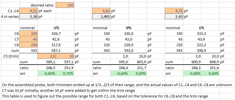
At the bottom, the spreadsheet calculates the resulting attenuation given the values for C1...C4 and C6...C8 (+trim). Since both trimmers were somewhere around their center, I wanted the resulting error at both ends of the trim range to be somewhat symmetric around zero (highlighted in green).
The left block shows the result for the case that C6...C8 were at their lower end (-1 %). To get into the right trim range, C1...C4 had to be set to 9.52 pF (top left). Similar for the center and right block.
Next step was to select a set of capacitor values that allow to build a probe where
- the "base" capacitance is known to be not too large for the lower end of C1...C4 and +1 % in C6...C8 (that's the one extreme of the overall spectrum)
- a maximum of 2 additional caps with known values can be added to get into the right trim range even for the upper end of C1...C4 and -1 % in C6...C8 (the other extreme) and all other combinations
- so no cap would have to be swapped - we'd just add more and know that it'll be good.
Some experimentation with the values made it obvious that these goals can't be achieved with just 3 footprints, so I added a fourth footprint to the next schematic and layout revision.
Good cap combo using values from the E12 series
The base values are 560 + 18 pF, and one or two 12 pF caps can be added.
For the low value of 9.52 pF for C1...C4:
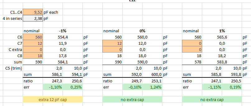
For the center value (9.62 pF):
for the upper value (9.72 pF):
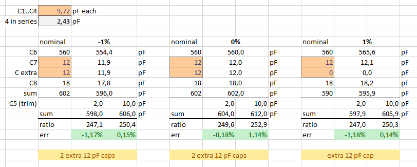
So during the compensation procedure I could start with just 560+18 pF, and add one or two 12 pF caps until the trim caps can do their job correctly.
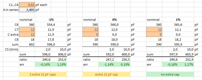
Good cap combo using values from the E6 series
Bud pointed out that he only uses E6 values. Well, since their spacing is wider, it's a bit harder to cover all cases. Starting with 330 + 220 + 33 pF, we can get very close and only one extreme case needs extra work if an extra 12 pF (yeah, that's E12 again...) isn't sufficient.
For the low value of 9.52 pF for C1...C4:
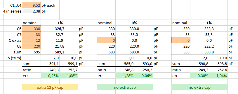
For the center value (9.62 pF):
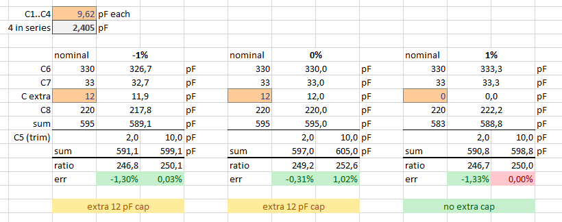
for the upper value (9.72 pF):
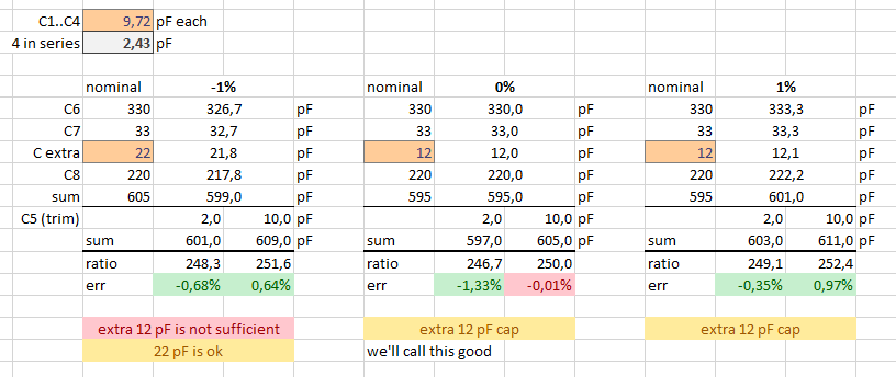
So only if C1...C4 have high capacitance and C6...C8 are low, we need more than 12 pF to get into the right range.
Aaaand given that the new layout will probably come with its own little intricacies, all this was probably pointless. But it was fun to bloat just one sample to this mass of numbers!
Next steps are
- wait for feedback on the current design's performance
- implement it
- order, build, test again.
(Attach current schematic - not built yet)
Discussions
Become a Hackaday.io Member
Create an account to leave a comment. Already have an account? Log In.
Good job, I like your writing style.
Are you sure? yes | no