 Christoph
The probe as it was designed by Bud and Paul works well and does the job. However, as always, there are ways to make it do more: Wolfgang was looking for a modified version that can connect to his keysight scope and make use of the scope's AutoProbe interface. Keysight scopes have an extra interface (a row of pogo pads below the BNC connector) that provides an I2C interface and supplies various voltages and an adjustable offset current to the probe. This can be used to supply the probe, auto-detect it, and set the offset. That's all pretty neat, but requires a couple of modifications on the probe and an external adapter that connects to the scope. The interface is described here:
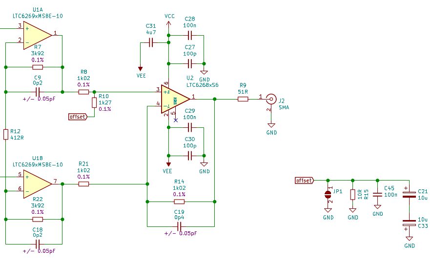
I found this quite interesting and started a design that can be used with or with the AutoProbe interface. I also wanted a more "pen"-shaped probe and Wolfgang suggested adding a white LED to the tip. Other modifications (starting off with Bud's 5V design):
- The spark gaps had to go, because they add extra input capacitance
- wider gap between the tip pads
- not a layout modification, but the clamping diodes D1 and D2 also add some capacitance that is not desired. They are not populated for initial performance measurements.
The modified probe needs a different external power supply if used without the AutoProbe interface, but that's not too hard to accomplish. It can now even be a simple 2S LiIon or LiPo battery, or a DCDC converter with +/- 5V output (those black blocky things)
Power supply
Power supply comes either as +/-12 V or as +/-3...6 V from the AutoProbe interface (some scopes apparently have +/-5 V only). This requires a different power supply on the probe. Instead of creating a virtual ground from a floating 5V suppky, we now have to create +/- 2V5 from the fixed dual supply with fixed ground. So I replaced the OpAmp that creates virtual ground by two low noise linear regulstor (TPS73125 and TPS72325).
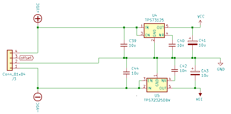
This part of the schematic also shows that the probe is connected to the AutoProbe adapter with a 4-pin connector.
Offset injection
The AutoProbe interface can inject an adjustable offset current limited to +/- 1 mA and a low voltage (5 V? not sure). This is sent through a 10R resistor at the bottom of R10 (instead of wiring R10 to ground). A 100 nF cap and a pair of tantalum caps were also added:
This allows the offset to be adjusted by +/- 1 mA * 10R = +/- 10 mV. That's just our first guess, and the offset resistor is large enough for comfortable rework (1206). It can also be left out and placed externally for experimentation.
Layout
Here's the new slim layout:
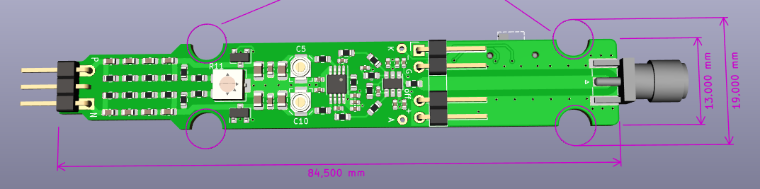
(84.5 mm x 13 mm)
The input header is a 3-pin header with the center pin removed, I was too lazy to modify the 3D model accordingly. Same for the 4-pin connector which can be a 5-pin type with the center pin removed. In this case I substituted for 2 2-pin 3D models because the 5-pin model would have obstructed the view of the output resistor that feeds the waveguide.
LED
The actual LED is not on the PCB, because that would have interfered with the attenuator layout. It's connected to a pair of through-hole pads (labeled "A" and "K") right next to the 4-pin connector instead, so it can be connected from either side of the PCB, depending on what would better fit the enclosure. There's a little switch in the back to turn it on and off.
SMA connector
The SMA connector is a bit smaller (6.35 mm wide) than the one on the initial layout (9.5 mm). It's also further away from the output OpAmp, so we added the waveguide you can see above
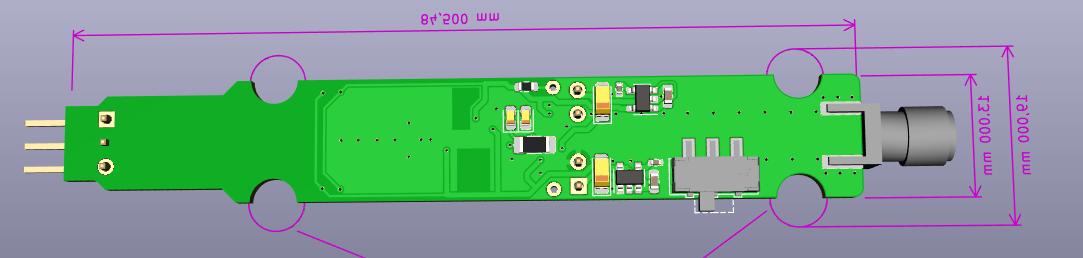
Other modifications
R8 and R21 were rotated by 45° to make the overall layout a bit prettier. Looks like a spider now.
The voltage regulators are on the bottom:
There are cutouts for threaded inserts in a 3D-printed enclosure. The threaded inserts on the input end would be a couple mm away from the attenuator, so hopefully they won't interfere with the measurement. On the other hand I'm not sure if a totally different enclosure concept might be better, but we'll figure that out.
Since this layout is new, I'll have to go through all the trial and error of finding the correct capacitors for the input attenuator again. The deviation from the theoretical values that Bud discovered is quite significant.
I also don't know if the ground layout is good enough, we'll have to measure the probe's performance to see what we have to improve, and how.
Design files will be published when we have assembled and tested one.
Discussions
Become a Hackaday.io Member
Create an account to leave a comment. Already have an account? Log In.
Hi,
thanks for this enhancement. Do you intend to publish the project and/or gebers files with BOM?
Are you sure? yes | no
Not yet - this design looked cool and all but the power supply really got in the way.
Sorry for the late reply, I didn't see the notification!
Are you sure? yes | no