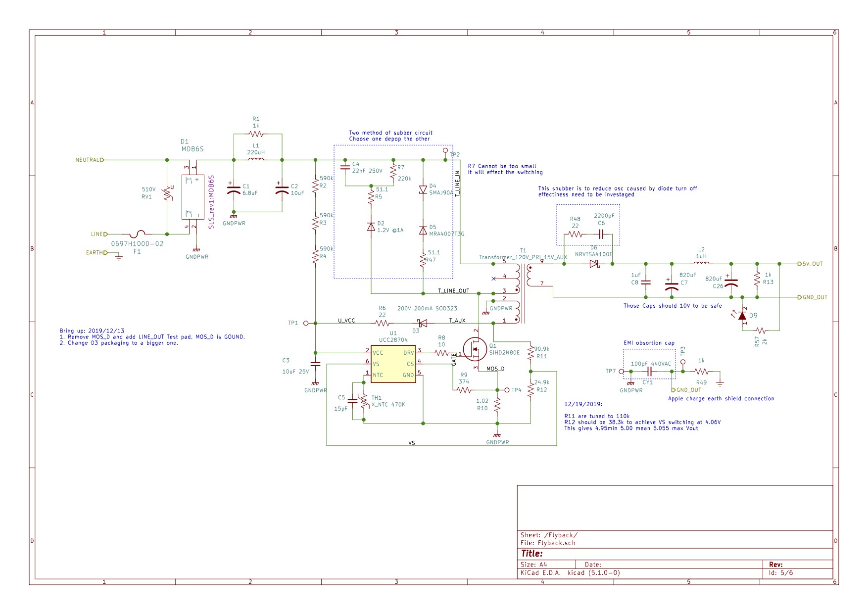
Here is the finalized circuit I have built and tested working for 120VAC. Let's go through the circuit component one by one.
Control chip
The control chip I used is UCC28704, which is a low cost and low part requirement chip from Texas Instruments. Highlight feature includes voltage valley skipping and no optical coupler required.
Voltage valley skipping reduces the ringing caused by the MOSFET switch turning off. Less voltage ringing would reduce EMI.
UCC28704 uses the AUX winding instead of the optical coupler to provide voltage feedback. Every stable system requires feedback. The Traditional and most common flyback converter uses an optical coupler to give control feedback from its output rail. This part does not have a long life and is often broken due to the optical part wear out fast.
Startup power of the chip
This is a smart way to power up the control chip by using a third set of windings called AUX windings. In my design, this would give out about 15V at AUX. However, when the system starts from zero, the aux would not have voltage since there is no switching yet, therefore, the chip needs to get its initial power directly from line input which is around 160VDC. This line voltage is reduced by a series of large resistors before feeding into the chip. Once it gets the initial juice to start operating the MOSFET, the AUX winding will start to have voltage and through a diode, only and a positive portion would be powering the chip now.
There is a more efficient way of this startup circuit. If the designer is aiming for higher efficiency to achieve a better power rating, for example, 80 plus Gold power ratting, one should consider this circuit to reduce start-up power loss and shorten the startup time. Instead of a series of resistance constant couple on the Vblk, a depletion-mode FET would connect the V blk when starting from no power and disconnect when ucc28704 is powered. This is controlled by one of the chips pin called NTC/SU, this would source a 105uA current when the chip is powered. Therefore, when the Qst2 has not current from the chip would result in qst1 be on. Vis versa. Detailed circuit please reference to 7.3.6.2 in the datasheet.
Regulation and feedback
Any stable system requires feedback to know if it is hitting its target. Without feedback, it would be blindfold and walking in the dark. Especially with an electrical system, without feedback, it would often result in a dramatic, loud and smoky outcome.
In this circuit, the feedback is done via the Auxiliary winding. Instead of an optical coupler, which has a low life cycle often fail before all other parts, Auxiliary winding will copy exactly behaviour as our output does, but with different voltage level. The controller chip will use this auxiliary reading to know to switch "harder" or idle for a brief moment. So that no overvoltage nor under-voltage at the output.
EMI
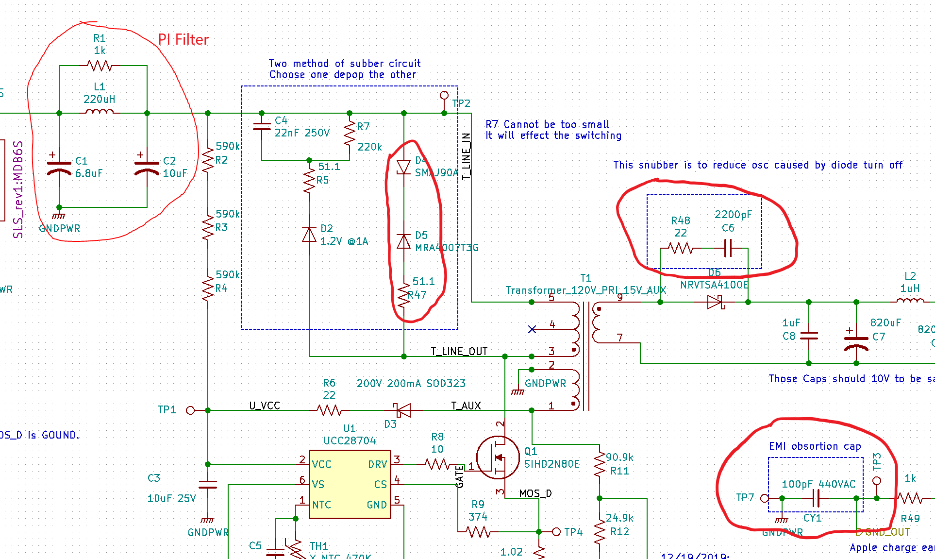
EMI is also a critical consideration when designing any power converter. In the circuit diagram, you will see Pi filters, Y capacitor connecting Power ground and output ground; snubber circuit to absorb the sudden change of voltage to reduce electromagnetic noise.
To be a commercialized product, all power converter has to pass Federal Communications Commission (FCC) in North America and CISPR in the European region.
The Pi filter I selected comes from a reference design of a similar 5V power converter. Since this stage I would not commercialize my board, I don’t have to go through lab testing on the effectiveness of my pi filter. Those emission tests require a radio frequency free environment and a lot of expensive equipment to achieve.
However, out of curiosity, I have some measurement on the effectiveness of the snubber circuit:
The Results show the TVS snubber circuit indeed drops maximum voltage peak on the line voltage after rectifier (Blue) from 736V to 352V and reduce 5V peak voltage from 5.8V - 5.55V ( This is before the 5V output target tuning so the output rail is a bit over 5V).
However, there is another interest found during the experiment. The snubber circuit would send the extra energy back to the T_LINE_IN node once the voltage peak over 350V. However, if we use a power resistor design, the resistance value can't be too small, i.e the peak voltage that the snubber circuit would age can not be set too lower. This would cause too much energy to send back to the Line Input and would disturb the UCC28704 switching behaviour and fail to maintain the output voltage.
Isolation
Isolation is great. It helps to slow down the spread of the virus during a pandemic but it also great for circuit designs. In general, AC lines usually carry a lot of high-frequency noise. This would get added to our DC output. A noisy power rail would also affect the normal operation of integrated circuits.
This is also a general great safety practice since you are dealing with AC. All downstream DC devices would not work well with 160V equivalent voltage nearby.
However, you still need to tie the AC Earth with your low voltage ground to make sure the low voltage ground is not offset from the true earth ground. If this happens, your device would have a higher electrical potential. If the metal casing/ any part of low voltage ground to touch other appliance that connects to the earth ground, a large amount of current would travel through the connection and cause damage to your circuit and a possible human user.
Here I connected the earth via a 1K resistor and tied power ground come out of the rectifier with a Y capacitor with my 5V ground. Later I could use the earth connect for the EMI shielding as well. This was inspired by an Apple Laptop Power tear down.
Discussions
Become a Hackaday.io Member
Create an account to leave a comment. Already have an account? Log In.