 James Wilson
As I began to think of a clock that would evoke the sense of time I had at camp, a few themes kept coming up. I had recently been introduced to bar Nixie tubes, such as the IN-9 and IN-12. By varying the amount current through the tube, you could change the length of the glowing segment. Their warm, retro glow were the perfect match for the time readout I wanted. I was also inspired by the minimalist industrial design of Braun desk clocks, from an exhibit on the work of Dieter Rams at San Francisco's Museum of Modern Art. Lastly, I wanted to power the clock from a USB phone charger. I was not yet comfortable with working with mains power directly, and my previous dabbling in Nixie tubes left me with an wasteful assortment of incompatible wall-wart power supplies. Since USB phone chargers were ubiquitous, I wanted to reuse them instead of contributing to more e-waste.
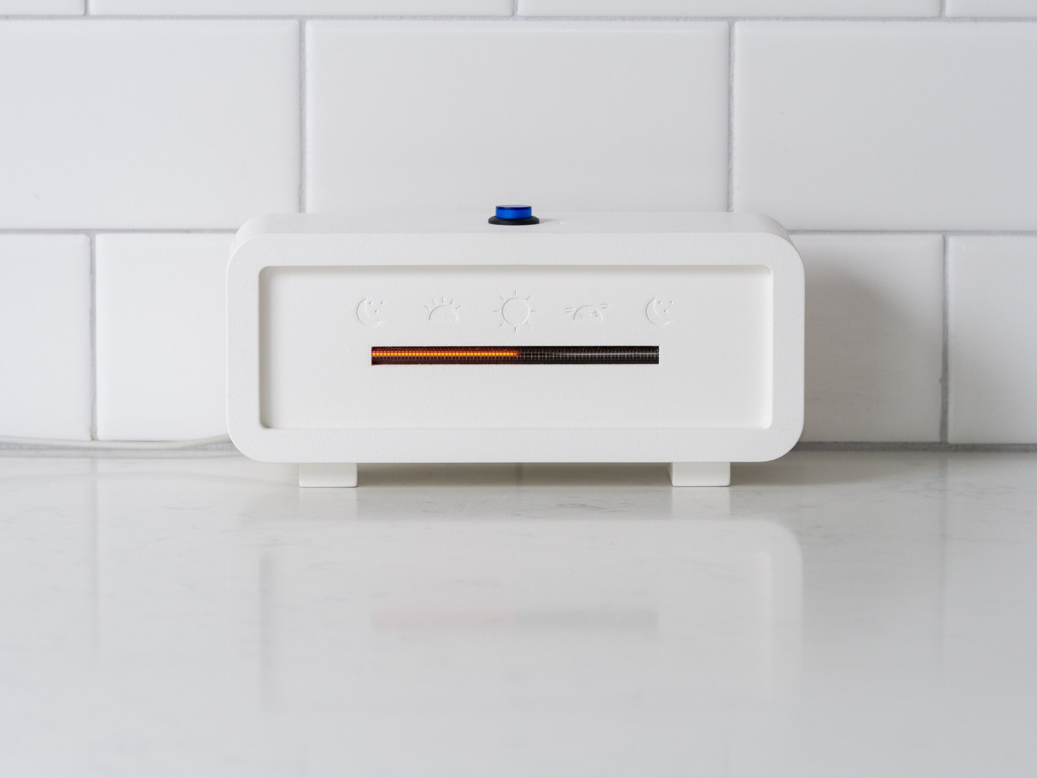
The project, "Leave Time Behind" takes the form of a desk clock. A custom printed circuit board (PCB) houses the main components of the electronics design: a switched-mode DC-DC power supply, a microcontroller with Bluetooth low-energy connectivity that keeps time, and a driver circuit that converts the digital time output from the microcontroller to an analog control signal.
The time is displayed on an IN-13 Nixie tube as a continuous glowing bar that grows longer over the course of the day. Compared to a traditional clock that allows us to obsess over hours and minutes, Leave Time Behind only permits the viewer to mark time and intervals approximately in relation to the natural cycle of the day.
When I thought of the design of the clock, I wanted it to have the minimum interface possible. In keeping with the aim to de-emphasize attention to hours and minutes, there are no discrete controls to set the exact time. To set the time, a single button on the top of the enclosure activates the Bluetooth function. When paired with a smartphone, the clock reads the time from the device.
The power supply
The power supply consideration ended up being the most difficult aspect of the design. Nixie tubes typically require an initial firing voltage of 150 to 170 V, with a sustaining voltage of around 100 V and current of a few mA. Stepping up USB's 5 V to about 150 V is no easy feat. I would need a DC-DC boost converter, and I couldn't find a ready-made design that supported in an input voltage of 5 V. I would have to design my own switching power converter. Every guide I read said that these circuits are not for beginners, but undaunted, I decided to try.
The first attempt at making a power converter was unsurprisingly a fiasco. How much inductance did I need? What size of output capacitor should I use? And what inspired these chosen R & C values for the controller compensation pin? Without a formal background in the theory of switching power supplies, I worked off of formulas in application notes and tried to fill the gaps with educated guesses. This would also be my first time designing a PCB for fabrication, so I had that additional learning curve. Amazingly, the first board "worked" in the sense that it produced about 140 V across the output with an open circuit and would light an IN-13 tube. But it was clearly not a great design; it couldn't source more than 2 mA without losing voltage regulation, and it was injecting a lot of nasty harmonics back into the input line.
The first test of the power supply lighting an IN-13 tube
This might have been a good point to punt and accept using a commercially available power supply, but something about the seeming wizardry of switching power supplies reeled me in. Over several months, I worked through a rigorous online course series (via Coursera/CU Boulder) on modern power converters, and came back to the project equipped to build something better. As I learned, trying to build a continuous conduction mode (CCM) boost converter with a conversion ratio of over 30 was a pretty bad idea. The best options for a better design were discontinuous conduction mode (DCM) boost or a flyback topology. I chose to go with DCM boost since I could use off-the-shelf magnetics instead of trying to source a transformer appropriate to the design. I also found a fellow experimenter who had tried to build the same thing (https://surfncircuits.com/2018/01/01/designing-an-small-footprint-low-profile-5v-to-170v-nixie-tube-power-supply-part-1/)! I traded a few emails with the author and pulled in some ideas from his design, such as the addition of a snubber in the power stage, but I was already pretty familiar with the LM3478 controller at this point, and wanted to stick with it.
The design I settled on converted 5 V to 150 V using a DCM boost topology, a switching frequency of 100 kHz, and maximum design current of 15 mA. This meant I could use surface mount inductors; the power stage inductor is a 15 µH surface mount device. Nixie tubes were designed to work with minimally-filtered rectified AC power, so I found a beefy 250 V C0G/NP0 .1 µF could achieve a 1 V ripple spec when driving a single tube at 5 mA. The following picture shows the iteration of board designs for the power supply. The last two boards were actually done after the completion of the clock project to explore additional filtering and soft-start additions to the design.
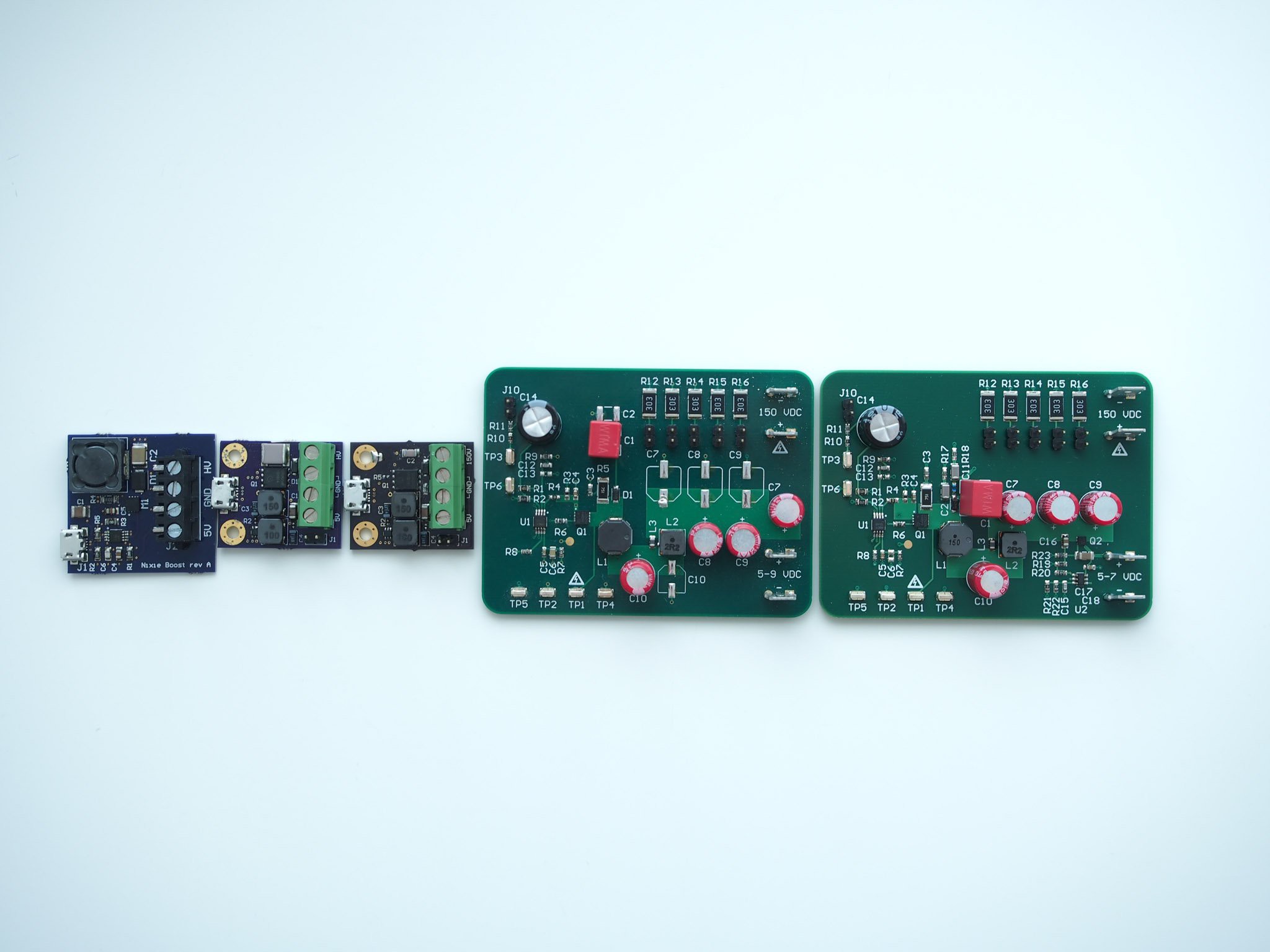
Revisions of the power supply evaluation boards. The later boards were designed after the completion of the clock project and include jumpers and components to add a DC load or test the controller's loop response.
The physical design and interaction
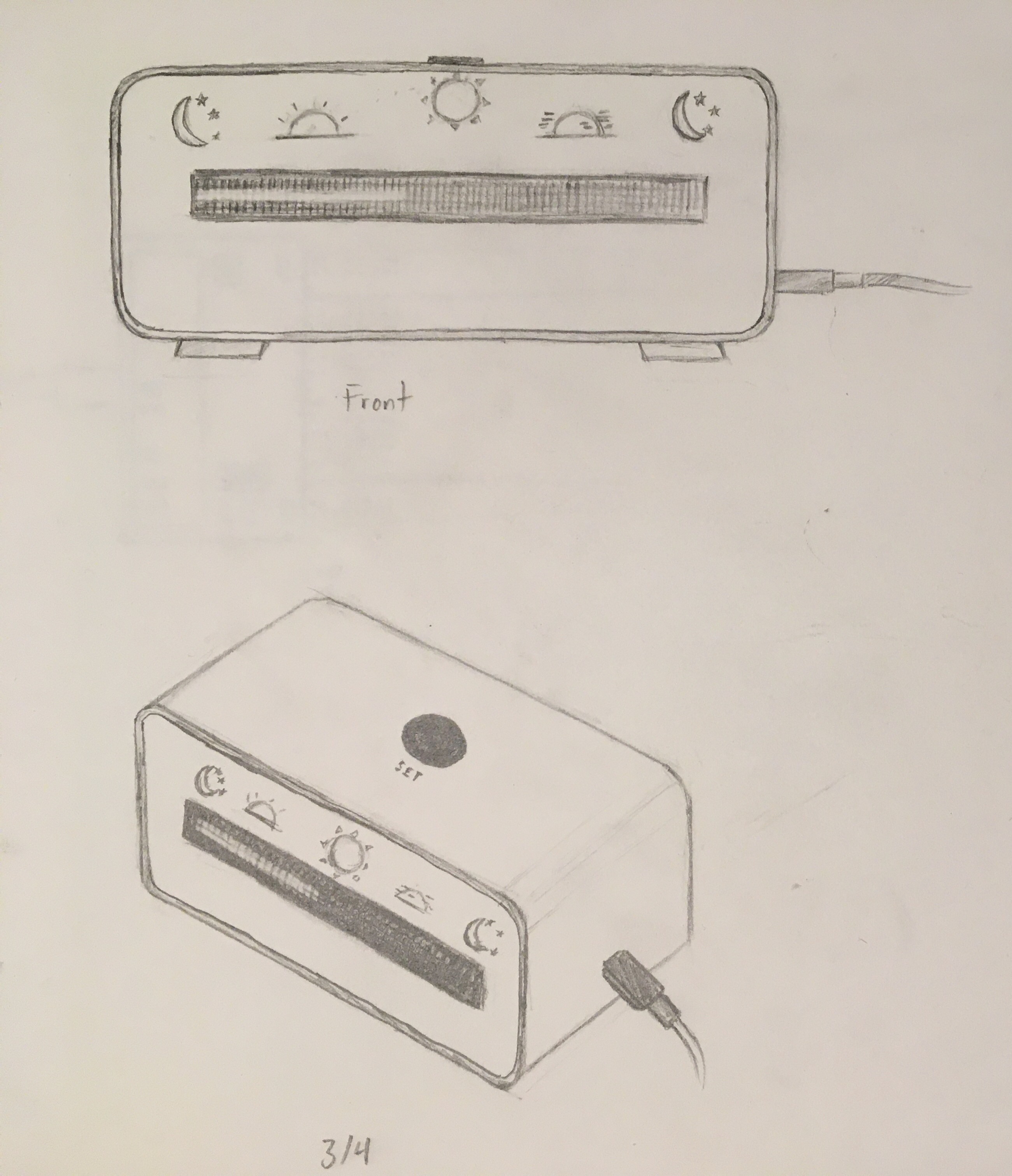 Early concept sketch showing the rounded rectangular frame and set time button
For the physical design of the clock, I was inspired by midcentury desk clocks, particularly from Braun. Dieter Rams' design philosophy was "as little design as possible." This presented an interesting problem for a clock that would not show exact hours and minutes: how should one set the time? Having discrete controls set the hour and minute would defeat the purpose of an approximate clock, and it would be impossible to show feedback on fine adjustments in the same way a minute hand would do. The answer to this question came after I learned that Bluetooth LE has a "Current Time Service" for setting device time. This service is basic enough that Apple implements the CTS profile in iOS. To set the time, I came up with this flow: the clock would incorporate a BLE microcontroller, and pressing a button on the clock would start BLE advertising. Once I connected to the clock from a phone app, the clock would ask for the time, update its RTC, and then disconnect.

Connecting to the clock in the nRF Connect app. Since the Current Time Service is built in to iOS, no special app is required. Any Bluetooth LE explorer app that connects to the clock will automatically set the time.
Next, I had to design the physical enclosure. I originally wanted to use wood to complement the warm aesthetic of Nixie tubes, but my lack of woodworking skills and access to equipment were an obstacle. I had already spent a lot of time teaching myself power electronics, so I decided to punt here and use a 3D-printed enclosure I designed in Autodesk Fusion. The enclosure has 3 parts: the frame, a front panel, and a rear panel. I glued the IN-12 Nixie tube to an cutout in the front panel, and the front panel is itself glued to the frame. The clock PCB assembly is mounted inside the frame, and the back cover with its cutout for a USB micro-B plug screws into the rear of the frame. For the front panel, I put some inset graphics showing approximate times of day: midnight, sunrise, midday, sunset, and night again. These would also look great if they were laser-etched in wood, but are also a nice subtle touch when inset in 3D-printed plastic.
The plastic case was printed using polyamide. The color was slightly translucent and off-white, so I applied a few coats of matte white spray paint with light sanding to get a smooth, brilliant white finish. The result matched my kitchen pretty well!
Tying things together: the microcontroller and PCB design
The clock required a microcontroller to manage three functions: communicating using BLE to get time from a phone or other source, keeping the current time, and producing an output signal that indicated how much of the day had elapsed, and would control how long is the lit section of the Nixie tube.
I turned to the familiar Nordic nRF5. Nordic semiconductor has great documentation of their SoCs with lots of example code. Conveniently, they have a "nrf_calendar" example that demonstrates the use of the Current Time Service to set the internal RTC; this code was cribbed to the build the code for the clock. I chose the mid-range nRF52832 since it has dual RTCs available. One RTC is used to keep the time, and the other is used for the PWM output driver. To display the time on the Nixie tube, the MCU outputs a PWM signal, where the duty cycle indicates the fraction of the day that has elapsed since midnight. The PWM signal is converted to a DC voltage level through a low-pass filter, which is then used as the control signal for a op-amp/MOSFET current source circuit that drives the Nixie tube.
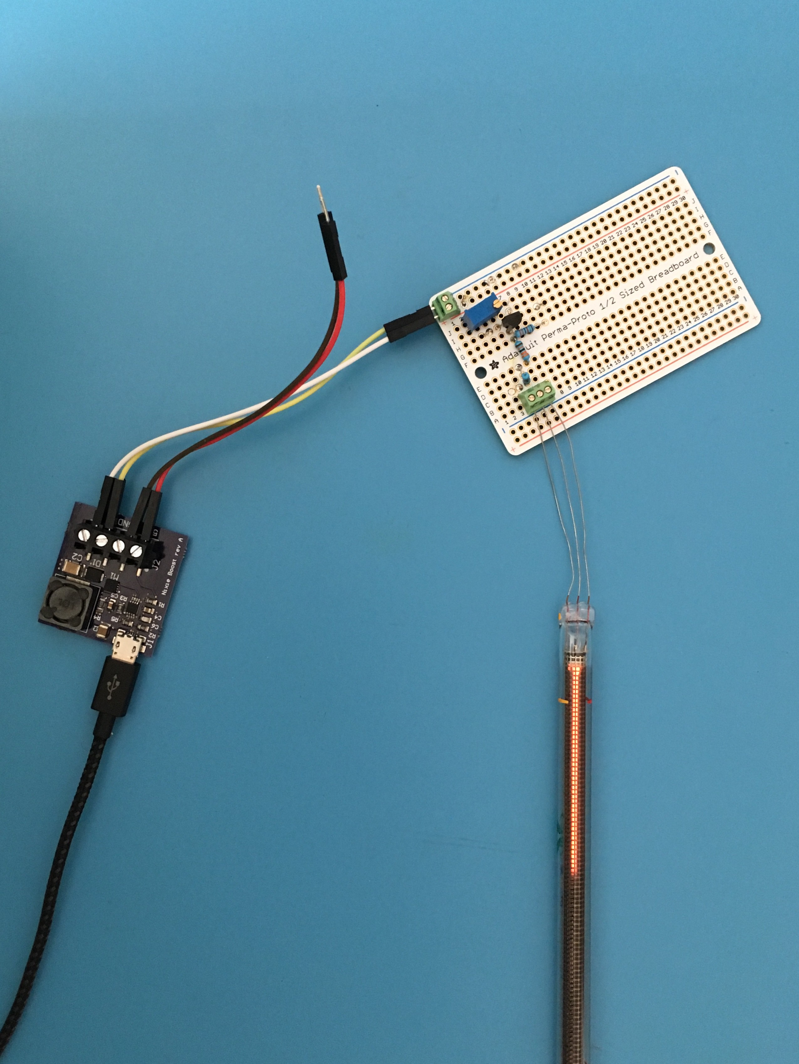
By now, I had cobbled things together using a Sparkfun nRF52832 breakout board and a breadboard to test the firmware. To fit everything into the enclosure, I needed a single PCB assembly that would put together all the parts of the design: the high-voltage power converter, the microcontroller for BLE and time keeping, an output driver to control the Nixie tube power from the microcontroller, and battery backup. To save some design time, I used a Rigado BMD-300 module that has the nRF52832 and PCB antenna.
The firmware code for the microcontroller, as well the PCB design files, are available on the project's Github repository (https://github.com/jmwilson/leave-time-behind/).

Breadboard prototype using a nRF52832 breakout board

Current revision of the PCBA for Leave Time Behind, highlighting the main components.
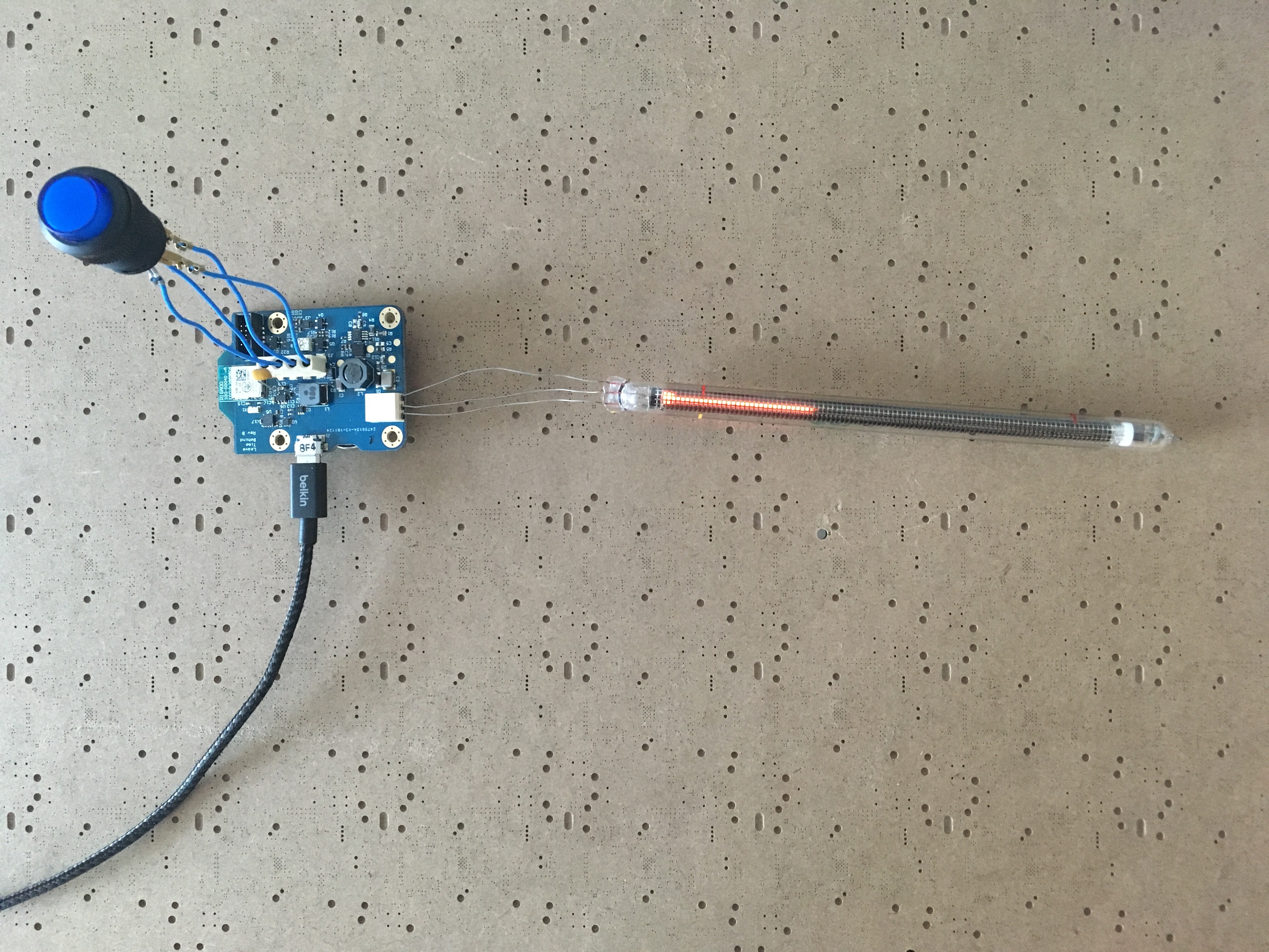
The PCBA for Leave Time Behind, showing connections from the headers to the Nixie tube and the control button.
Future Directions
Since I built Leave Time Behind, it's been a constant companion on my desk. Schedules, events, and appointments mean I still have need of the precise time of day, but every now and then it's all the clock I need. I have considered how I might improve the design still. The first idea would be to add a GPS module to simplify setting the time. Instead of getting the time through BLE and a smartphone, GPS could set the time with no interaction at all! The current time is sent through the GPS protocol, and lat/lon data could be used to calculate the local sunrise and sunset time. You wouldn't even need to adjust it for a road trip or daylight saving time - the sun doesn't care about us setting clocks ahead or back twice a year!
In continuing with this project as a learning platform for power electronics, now that I have done other projects and am more comfortable with the idea of working with mains voltage, I could also replace the DC-DC power supply with an offline SMPS that would rectify AC and step it up or down as needed for the Nixie tube and the low-voltage digital components.