 Yann Guidon / YGDES
See at the bottom for a slightly better version
This circuit shows a variation on the one presented in the first log :
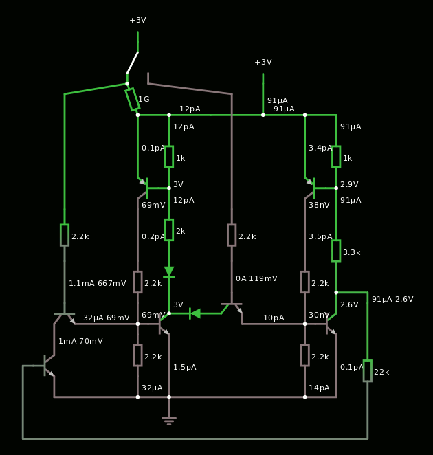
This shows the "SCR slices" linked by two NPN "pass gates". The output is looped back to the input with an additional NPN.
So it is possible to have two configurations :
- either 3 PNP and 3 NPN per DFF, or
- 2PNP and 4 NPN.
The choice depends on the availability of the transistors, and influences the clocking scheme : using "NPN pass gates" only requires the creation of two independent non-overlapping pulses per clock cycle.
Apparently the clock system will be a whole problem in itself...
Here is the source code :
$ 1 1e-9 1.2182493960703473 66 5 43
g 672 432 672 464 0
w 624 144 624 224 1
w 624 320 528 320 3
w 624 128 624 144 2
w 624 320 624 336 0
w 640 320 624 320 0
w 672 272 672 304 2
w 624 400 624 432 1
w 624 320 624 288 2
w 672 432 624 432 0
w 672 336 672 432 1
w 672 112 656 112 0
w 672 96 672 112 2
w 624 0 624 96 1
w 624 0 672 0 0
w 672 0 672 32 1
w 672 112 672 144 1
r 672 144 672 208 0 2000
r 624 224 624 288 0 2200
r 672 32 672 96 0 1000
r 624 336 624 400 0 2200
t 656 112 624 112 0 -1 2.930529235861507 -1.1867824944999938e-8 100
t 640 320 672 320 0 1 -2.9305256619877182 0.06947075183066788 100
r 512 144 512 224 0 2200
t 512 288 512 320 1 1 0.5968215934651058 0.5973307394672914 100
w 496 432 624 432 0
w 512 -32 512 144 0
w 512 224 512 288 3
d 672 208 672 272 2 default
d 752 304 672 304 2 1N4148
w 928 272 976 272 0
w 976 496 448 496 0
w 768 224 768 272 3
w 736 0 816 0 0
w 768 -32 768 144 0
w 816 0 816 -48 1
w 672 432 880 432 0
w 784 304 784 320 0
t 768 272 768 304 1 1 -2.8805655700300177 0.11937009322376849 100
r 768 144 768 224 0 2200
t 896 320 928 320 0 1 -2.607606715813171 3.037300559797447e-8 100
t 912 112 880 112 0 -1 2.908745716789634 -0.09125424512435565 100
r 880 336 880 400 0 2200
r 928 32 928 96 0 1000
r 880 224 880 288 0 2200
r 928 144 928 272 0 3300
w 928 112 928 144 1
w 928 0 928 32 1
w 880 0 928 0 0
w 880 0 880 96 1
w 928 96 928 112 2
w 928 112 912 112 0
w 928 336 928 432 1
w 928 432 880 432 0
w 880 320 880 288 2
w 880 400 880 432 1
w 928 272 928 304 2
w 896 320 880 320 0
w 880 320 880 336 0
w 880 128 880 144 2
w 880 320 784 320 1
w 880 144 880 224 1
w 816 0 880 0 1
w 672 0 736 0 1
R 816 -48 816 -80 0 0 40 3 0 0 0.5
S 624 -112 624 -48 0 1 false 0 2
R 624 -112 624 -144 0 0 40 3 0 0 0.5
w 608 -48 512 -32 0
w 640 -48 768 -32 0
t 464 384 496 384 0 1 0.5300334614902087 0.6000133593230622 100
w 496 320 496 368 3
w 496 400 496 432 0
r 976 288 976 496 0 22000
w 448 496 448 384 0
w 448 384 464 384 0
r 608 -48 624 0 0 1000000000
w 976 288 976 272 3
o 2 4 0 4355 1.25 0.0015625 0 2 2 3
o 6 4 0 4354 5 0.1 0 2 6 3
o 31 4 0 4354 0.625 0.0015625 0 2 31 3
o 31 4 0 4355 0.625 0.00009765625 0 2 31 3
o 60 4 0 4355 1.25 0.0015625 0 2 60 3
Here is a slightly optimised version, one diode less, less current, using only 2K2 and 4K7 resistors.
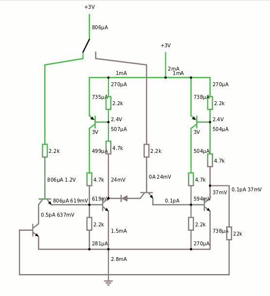
current on the GND node doesn't exceed 2.8mA, cycles through
1.1mA 1.8mA, 2.8mA, 2mA
Base resistors are all 2K2. 4K7 connects the complementary sides to reduce the curent.
This circuit also shows how to "drive" the first element of a shift register : with a simple pull-down transistor.
Discussions
Become a Hackaday.io Member
Create an account to leave a comment. Already have an account? Log In.