 Tim
Tim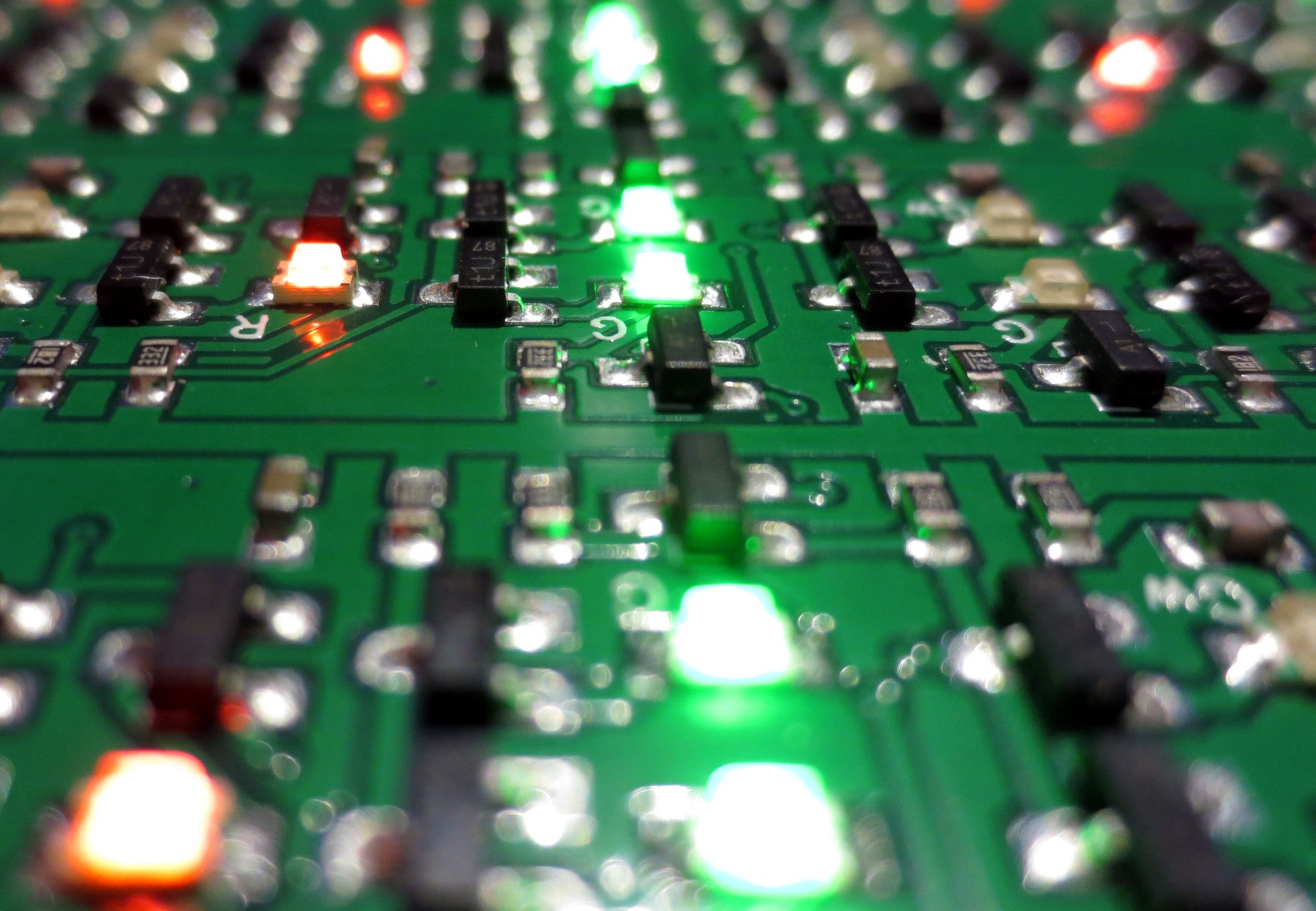 Above you can see the an image of the hardware while it is operating. The red LEDs are part of the low threshold gates in the latches, while all other gates use green LEDs to set the threshold to ~2.3V.
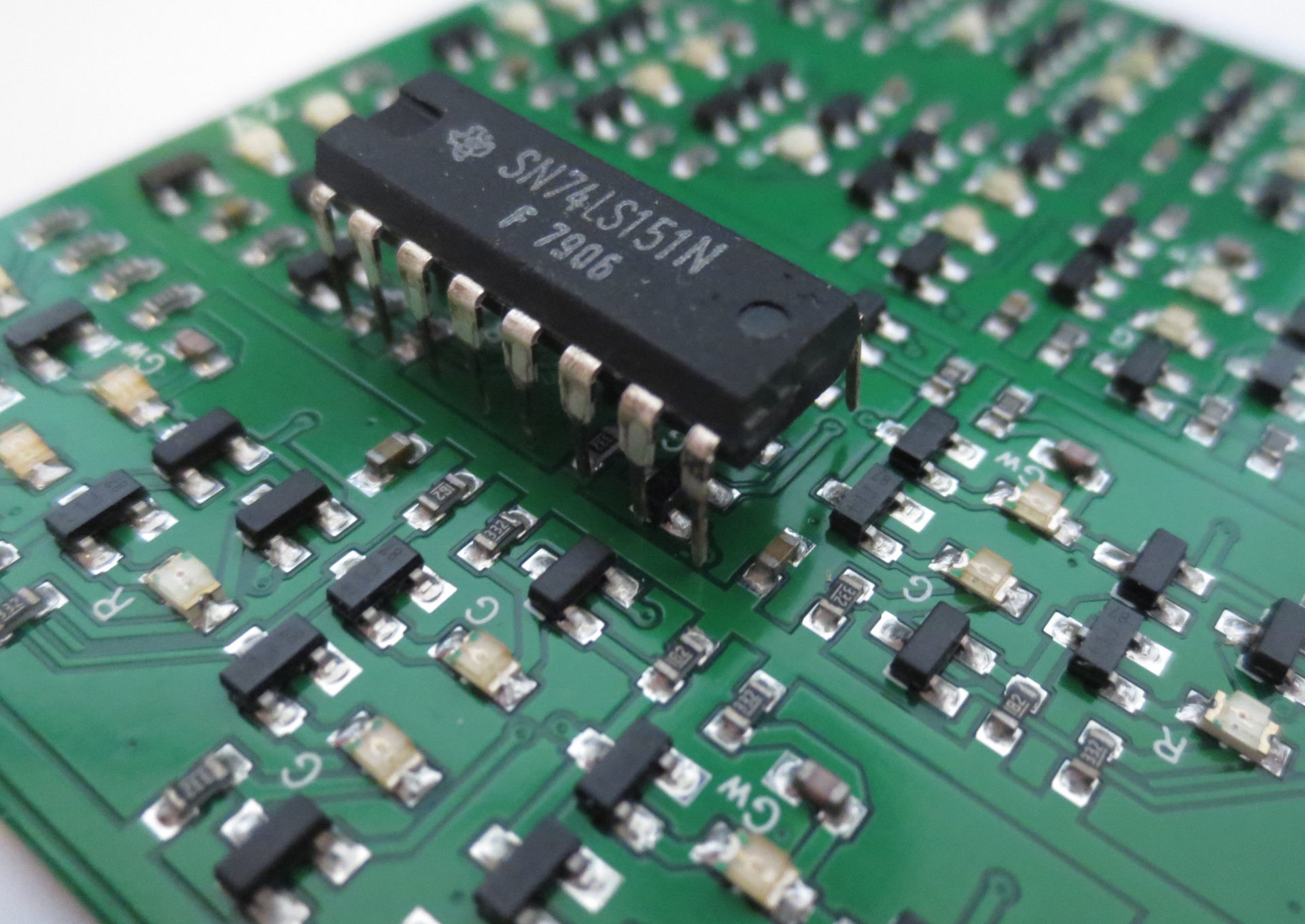 A size comparison with a TTL ICs. The gate density on the PCB in NAND equivalants is slightly lower than what would be achieved with 7400 NAND gates. Something to be addressed for later iterations...
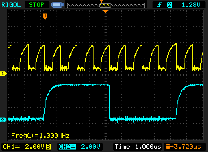
The scope image above shows the A0 and A2 output of the address unit with SEL_DATA=0 and SEL_PC=1. In this configuration, the PC is increased with every clock cycle. Here, a clock of 2 MHz clock was applied. Operation was also successful at 4 MHz. I was not able to test any higher due to limitations on the generator side. Obviosuly this would reduce when more 4 bit slices of the adress path are combined, because the length of the carry chain would increase. One can see from the signal shape that the operating speed is very much limited by the rising edge. Right now, the collector current is limited to 2mA. Increasing the collector current further would allow even higher clock rates at the expense of power. Introducing push-pull output drivers may also be an option.
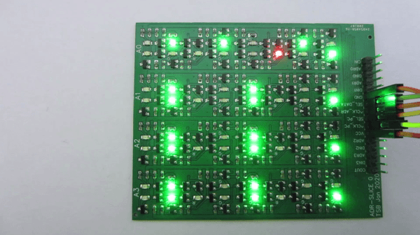
Finally some blinking action, clocked at 2 Hz! Higher resolution here. The red LEDs on the left side of the PCB indicate the state of the address lines and are not part of any gate. You can see how the PC is counting up.
Btw, only after looking at this animation, I realized that the fast (red) gates actually reflect the output state of the latch, even though they are not connected to the output. So, next time I can omit additional indicator LEDs.
Discussions
Become a Hackaday.io Member
Create an account to leave a comment. Already have an account? Log In.
It looks delicious :-)
Are you sure? yes | no