 land-boards.com
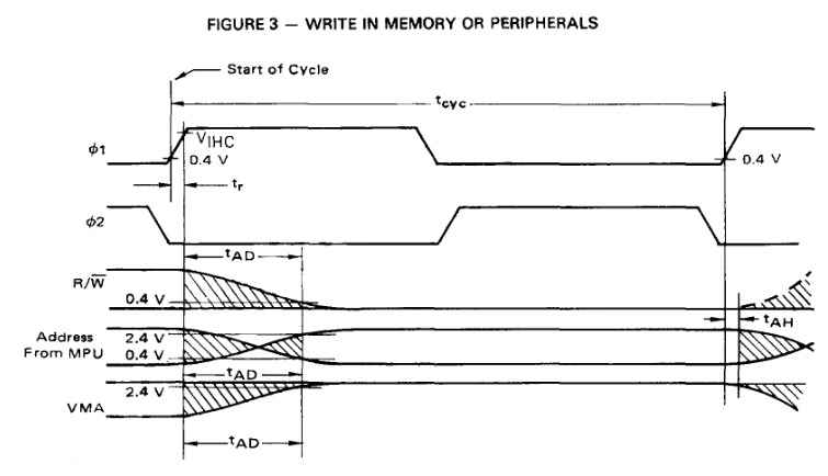
One of the nicer things about the 6800 FPGA core is that it doesn't need a dual phase clock. However, the operation of the clock is not particularly well documented for the FPGA core. At the very least there's no comments in the code that explain the clock operation. To get an idea what is going on we will have to take a look at the VHDL code. The typical use in the VHDL code for the cpu68 core looks like this:
if clk'event and clk = '0' then
This usage leads me to think that the falling edge is the start of the cycle. All uses of the clock follow the same falling edge style. This makes me conclude that the clock is the equivalent of the Phase 2 clock from the data sheet.
The equations for the active low write strobe that seem to work are like this:
n_WR => n_if1CS or w_R1W0 or (not w_vma) or (not w_cpuClock),
The sense of this equation feels backwards at first but basically if read in the negative it says something like:
De-assert write strobe when not chip select OR when read OR when not VMA or when not clock.
Flipping this around - assert write when chip select AND write AND VME and CPU Clock. That also corresponds to the Phase 2 clock high.
If anyone has better knowledge, feel free to comment.
This is in contrast to the MC6502 CPU (T65) core which is rising edge driven so any example VHDL code for the 6502 will need to use the other edge.
Double Strobes
I've seen some effects which seem like double strobes when I've messed around with these signals. This is particularly a problem when the CPU speed is increased. The CPU may be too fast, but the Buffered UART and VDU interfaces work with other faster Multicomp designs so I'm skeptical that is the issue. Grant didn't publish a 6800 reference design so we are somewhat on our own here.
Discussions
Become a Hackaday.io Member
Create an account to leave a comment. Already have an account? Log In.