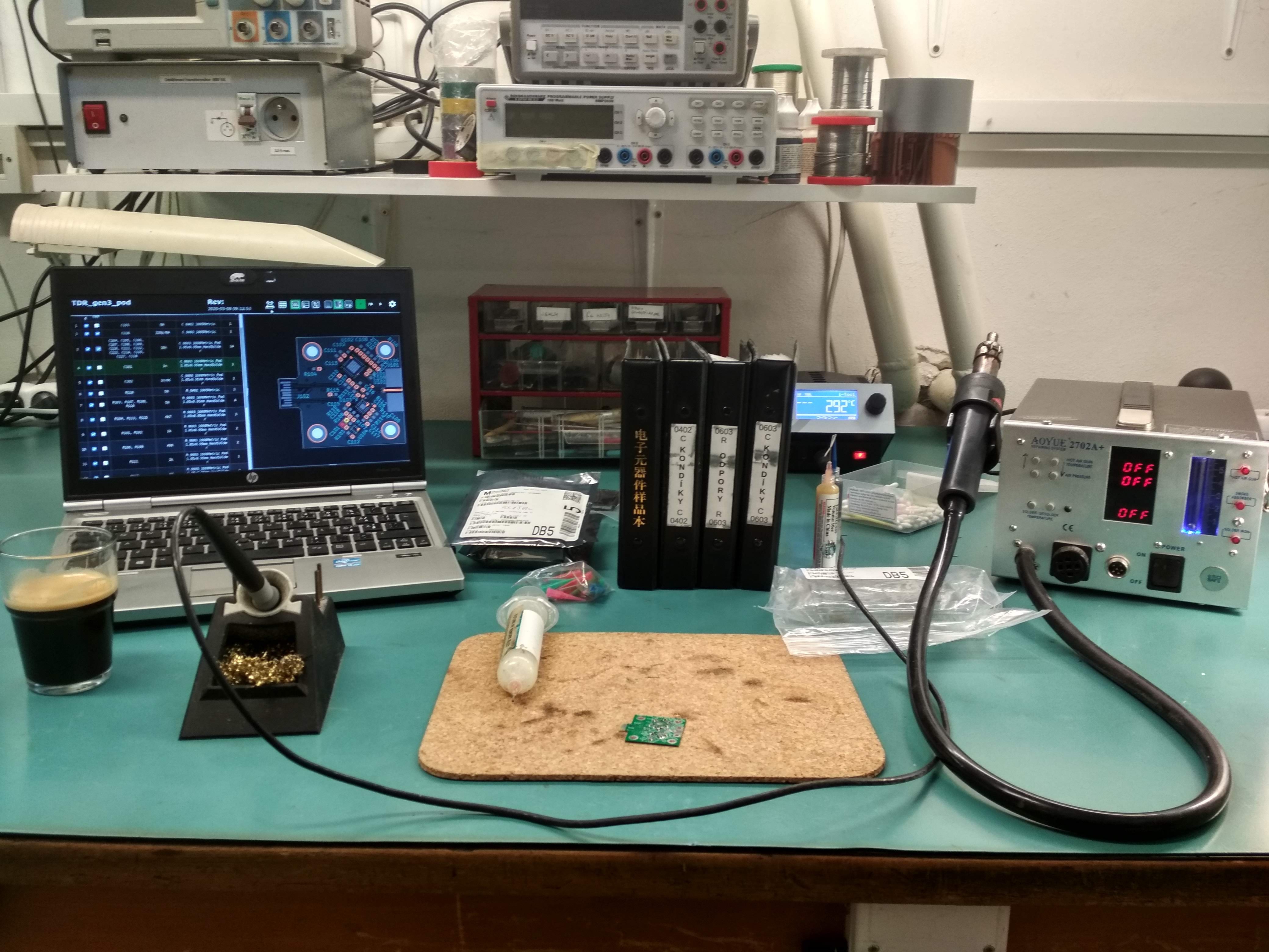
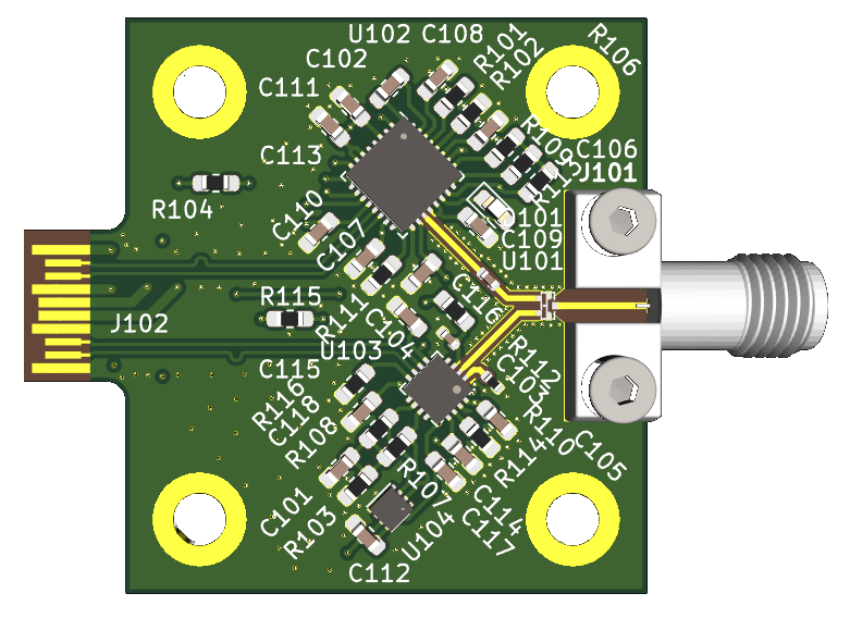
 MS-BOSS
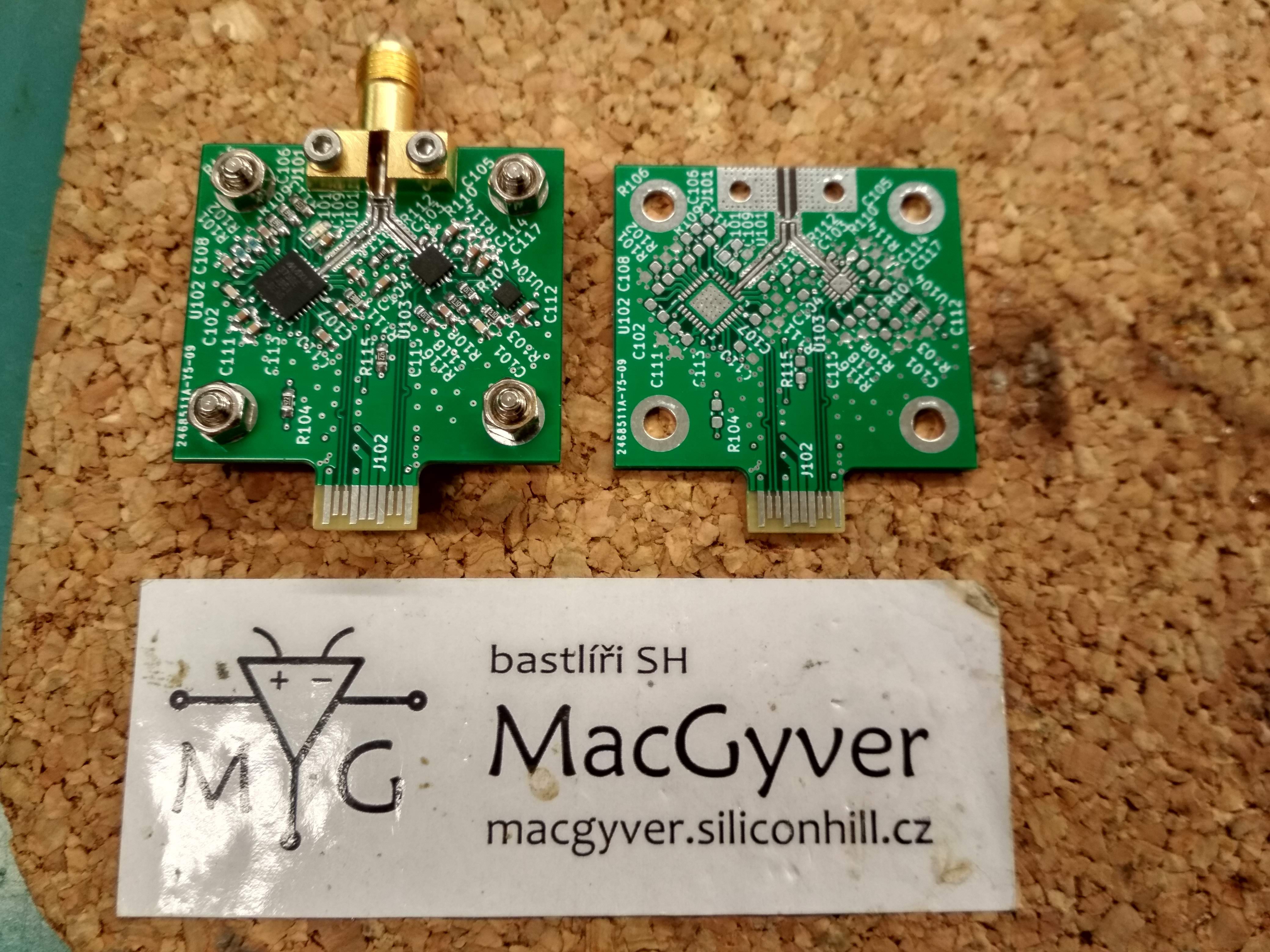
The "pod" contains MAX3798 for pulse generation. The datasheet promises 26 ps risetime into 50 Ohm termination. Its modulation current can be programmed in 512 steps thus allowing for changing the output power of the generator.
The generated pulses are fed into resistive network (special three terminal resistor for this purpose) and then into DUT. The mix of incident and reflected impulses are fed back through the resistive network into ADCMP582 which serves as sampler.
The PCB fits into SFP+ socket. By building a main PCB with 2 pulse generators with variable time offset and one DAC, this can be a complete TDR. By converting its output to frequency domain, it can serve as crude VNA able to measure S11 parameter When using two pods, it can serve as both TDR and TDT. Because both are complete transceivers, it is possible to use a device with 2 of these pods as full 2-port VNA, which can measure S11, S21 and also S12 and S22.
 The problematic solder pad after being already solved (the leftmost one at the bottom row).
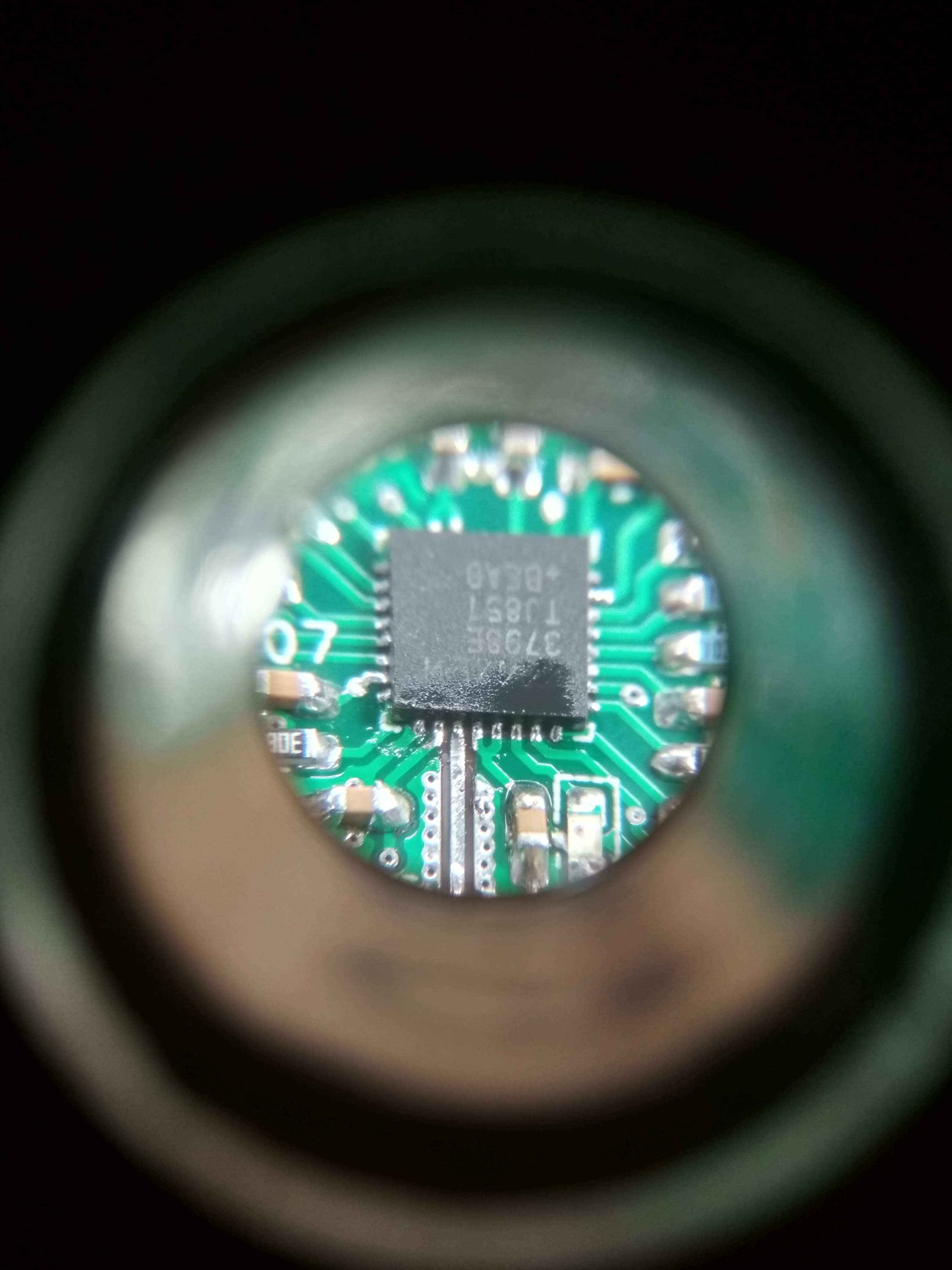 Cleaning in IPA in ultrasound cleaner:
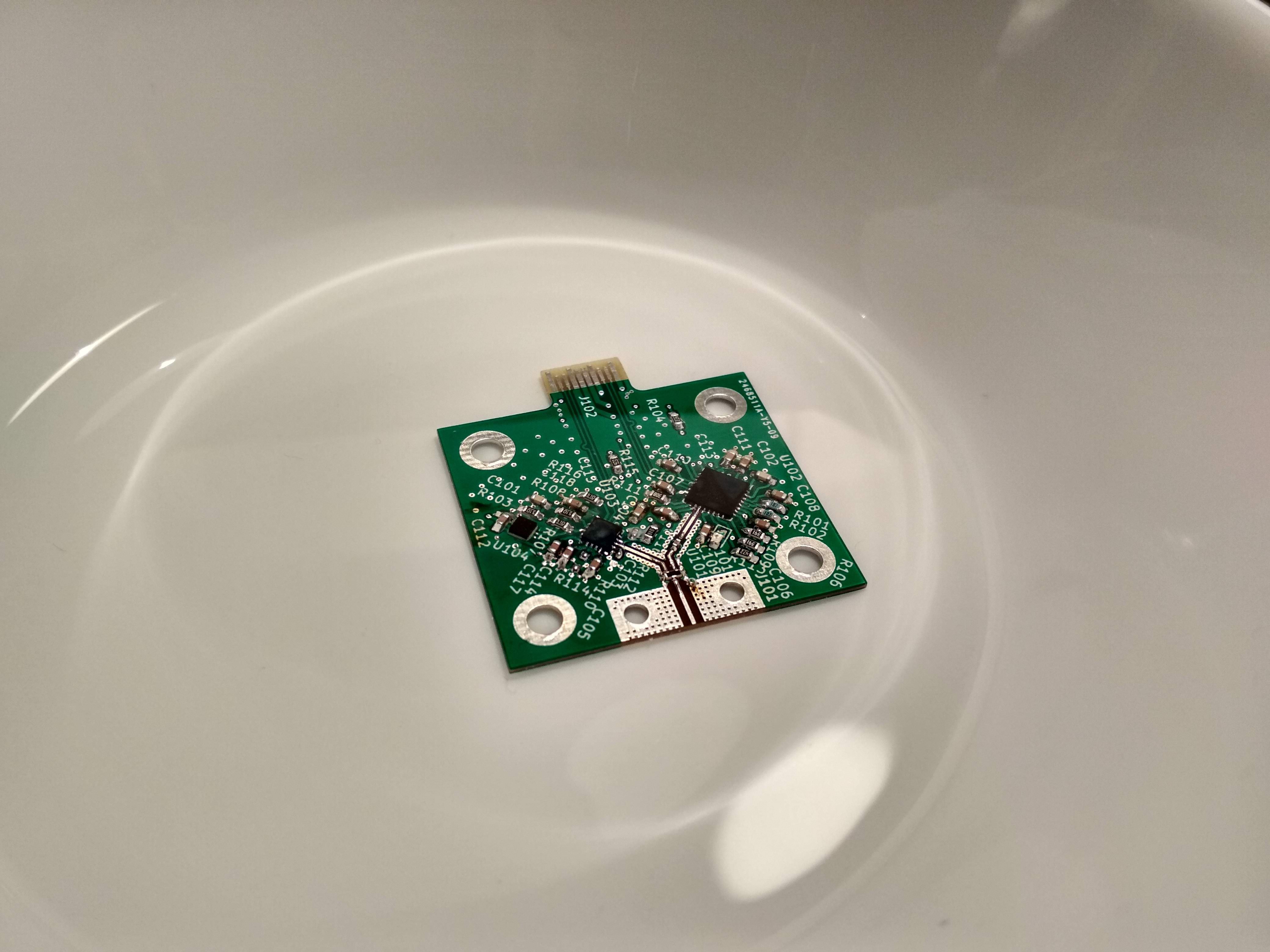


 Simon
Simon
 Kevin Neubauer
 Martijn
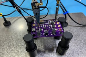
 tonyo
tonyo
I currently work on creating a simple IR-UWB radar and this project requires the generation of gaussian pulses around 130 ps. The MAX3798 looks like a cool alternative to the classical SR diode pulse generators or logic glitchers. Can you say, which rise times and amplitudes you achieved with your design?