 MorriganR
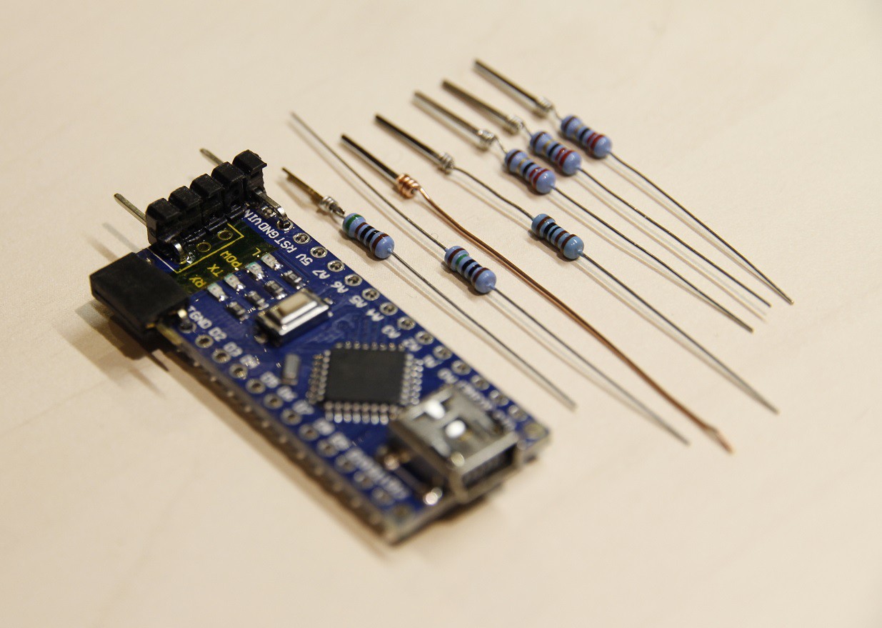
In my opinion, the most appropriate name for this project is JTAG Hello World because it implements the IEEE 1149.1 basic standard. From which the minimum set of functions was used. JTAG was implemented using bit-banging technology. This allowed the entire project to be executed on an Arduino board with a minimal number of additional components. A similar project can be found at https://github.com/alexforencich/ftjrev.
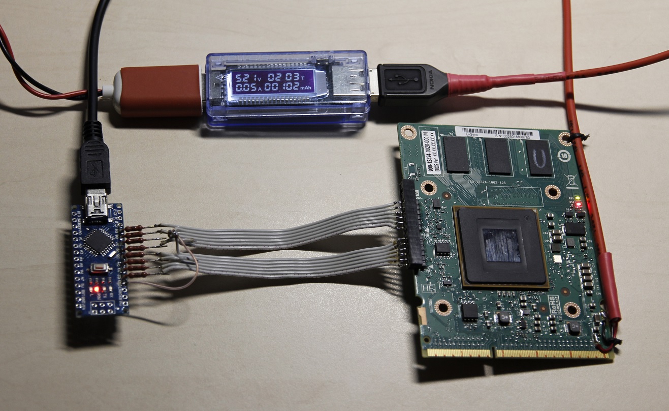
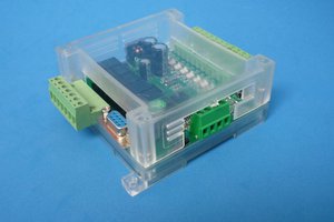
Hardware
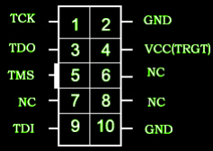
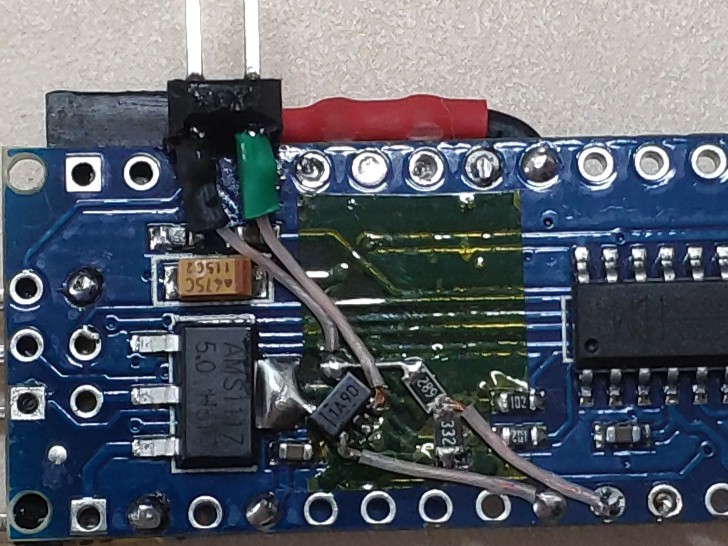
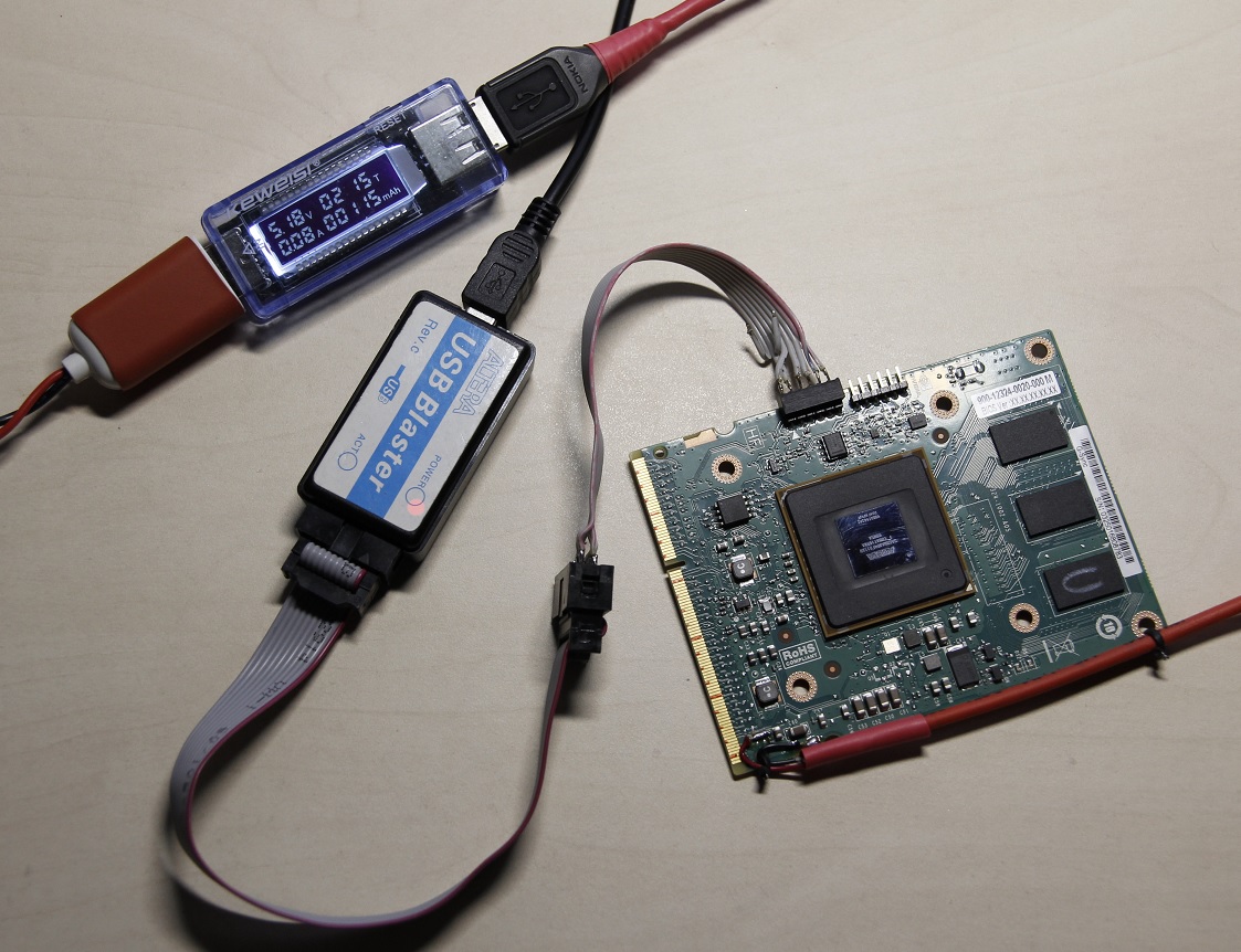
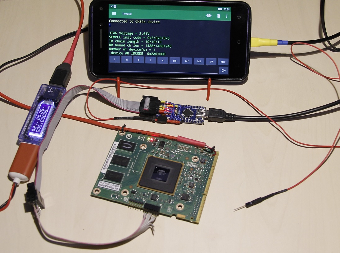
See BUILD INSTRUCTIONS for more information. The device has an Altera USB Blaster-compatible JTAG connector.
Software
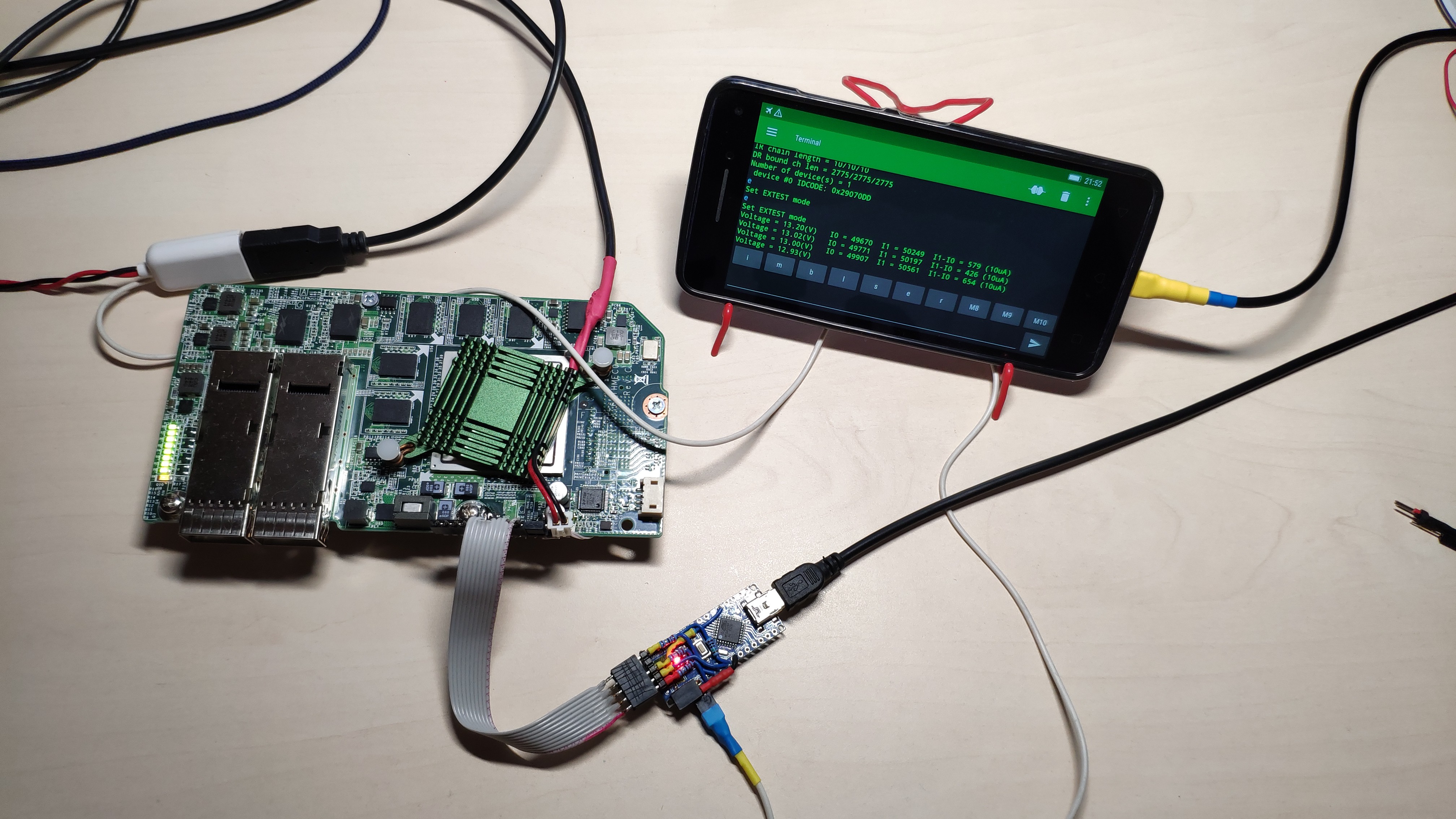
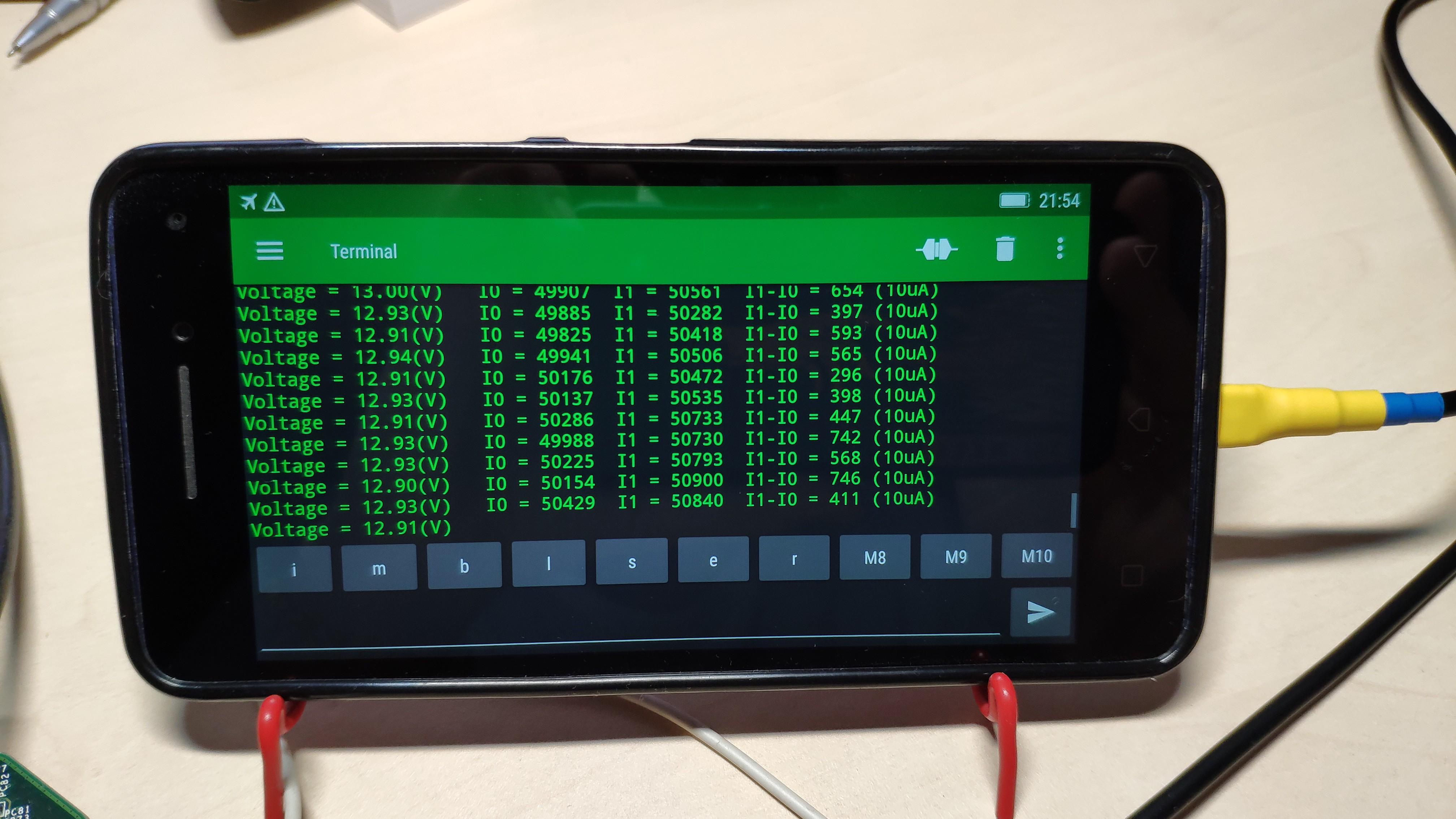
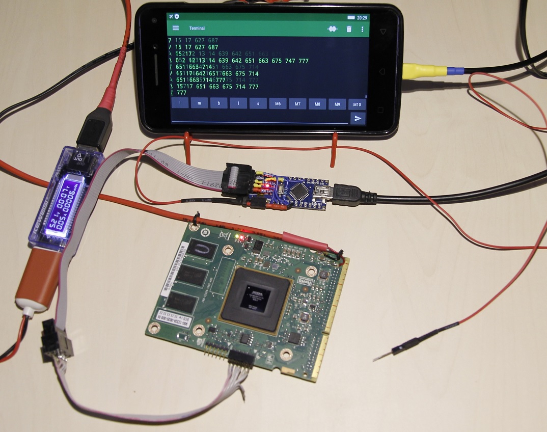
All software is an Arduino script. A terminal such as Putty or Serial USB Terminal for Android can be used to display the information. The block diagram of the code is shown below.
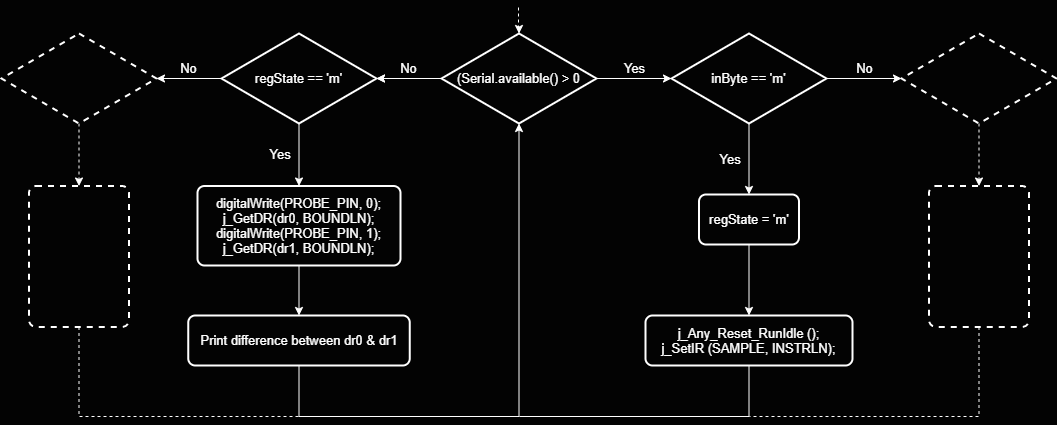
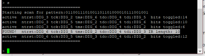
The flowchart shows the algorithm of the function 'm' (Monitor), which corresponds to the function Input probing in the project ftjrev.
TAP state machine
SAMPLE
The easiest way to understand how the algorithm works is by looking at the diagram of the TAP state machine. The figure below shows the algorithm of work of the SAMPLE command.
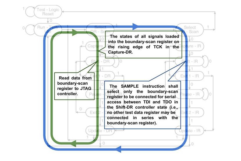
Once passed the blue path, we enter the code of the SAMPLE command in the instruction register. After that, the boundary-scan register will be set as the data register. In the future, we do not need to constantly enter the SAMPLE command code in the instruction register, it will remain there until it is overwritten by another instruction or is reset by entering RESET state.
After that we can constantly move along the green circle, in meanwhile, reading the state of the pins from the boundary-scan register. In accordance with the Standard, upon exiting the Capture-DR state, data on the state of the pins is transferred to the boundary-scan register, which can then be read in the Shift-DR state.
EXTEST
The algorithm of work of the EXTEST command is very similar to the algorithm for working with SAMPLE, but with some exceptions.
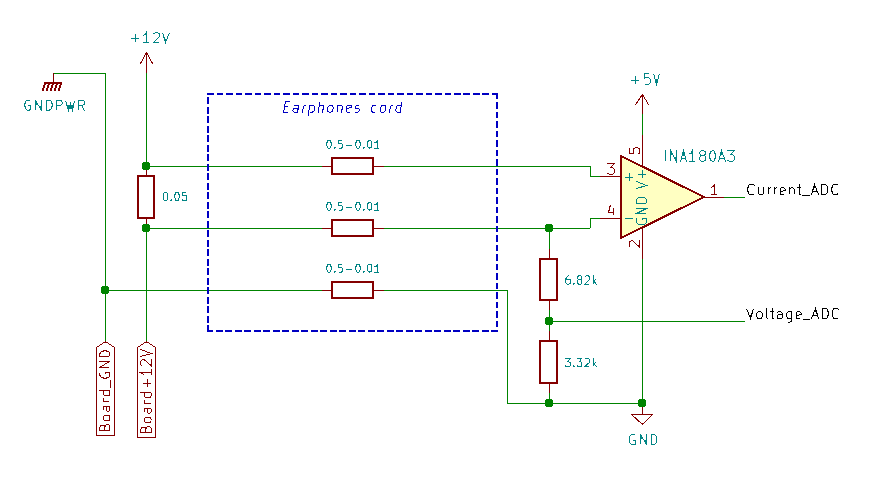
First of all, it is crucial to remember that working with an EXTEST command without knowing the electronic schematic is not safe. Using EXTEST allows you to set the pin to state 0 or 1, while this pin can be connected to the output pin of another chip, as a result we can get significant currents through these pins. It is unlikely that this will lead to an instant failure, but you should not leave the system in this state for a long time.
As in the case of SAMPLE, at the beginning, we need to enter the EXTEST command code in the instruction register, this is shown with the yellow path in the figure below.

Here comes the other thing, in accordance with the Standard, the pin levels are set to the state, which is defined with the boundary-scan register on the falling edge of the TCK in Update-DR state. But when we just entered the EXTEST command code into the instruction register (presumably in the Update-IR state), the state of the pins should already be determined by the contents of the boundary-scan register. So before entering the EXTEST command into the instruction register, it is highly advised to initialize the boundary-scan register with a safe value using the PRELOAD command, which will keep all the pins in the Z-state. Its code usually matches the code of the SAMPLE command.
It sounds too confusing, but the pseudocode of initializing EXTEST looks pretty simple:
j_Any_Reset_RunIdle();
j_SetIR(SAMPLE, INSTRLN);
j_GetDR(dr2, BOUNDLN);
j_SetDR(dr2, BOUNDLN);
j_SetIR(EXTEST, INSTRLN);
In this case, we assume that the value stored in the dr2 array after executing the SAMPLE instruction contains the safe value for the boundary-scan register.
In the future, we can move along the red path reading the status of the pins and controlling them as shown...
Read more »


 alberto nunez
 Just4Fun
 Dave Vandenbout
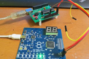
 kodera2t
Very interesting project, but I could not infer the theory of operation or usage from the .ino, and the video has no sound so it also did not help in understanding. Will you be elaborating how to use?