 MorriganR
This document describes the work algorithm of the JTAG Knock-Knock(Device). All experiments were performed with a G-Sync board containing an Intel Arria V GX . The first few steps do not describe the actual usage of the Device, instead they do explain preparatory steps.
Step 1
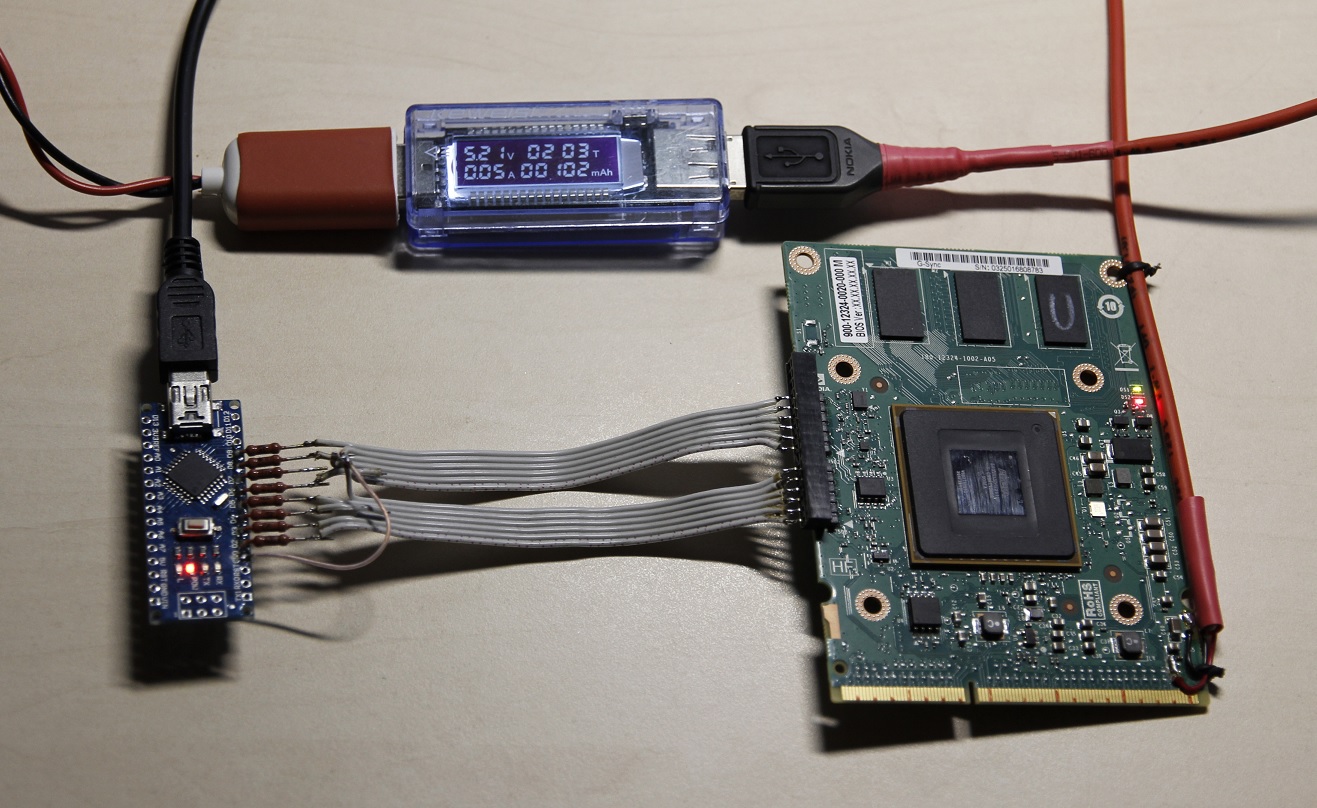
To actually start working, it is needed to determine the placement of the JTAG port on the board. First thought was about two connectors on the end of the board, that has 6 pins each, that is the one we are going to check. With a regular tester it is not difficult to determine which pins in connected to the ground. Unfortunately, it is not enough to deal with other pins. Since it is not the purpose of the Device, JTAGenum was used. Click on the link, in order to find detailed instructions on how to use it and the Arduino sketch code. Connect Arduino to the board to start searching for JTAG pins.
After just a few seconds of functioning we see the following result in the terminal:
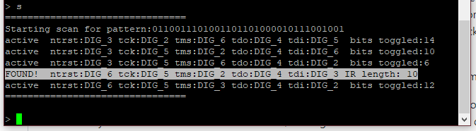
The line we need is highlighted with white. That so conformity of JTAF signals and physical pins is found.
pin 1 - TMS
pin 2 - TDI
pin 4 - TDO
pin 5 - TCK
Step 2
Using the information from the previous step, it is possible to make a cable to connect USB Blaster easily. Now connect the USB Blaster to the board and make sure that the Quartus Programmer sees the FPGA installed on the board.
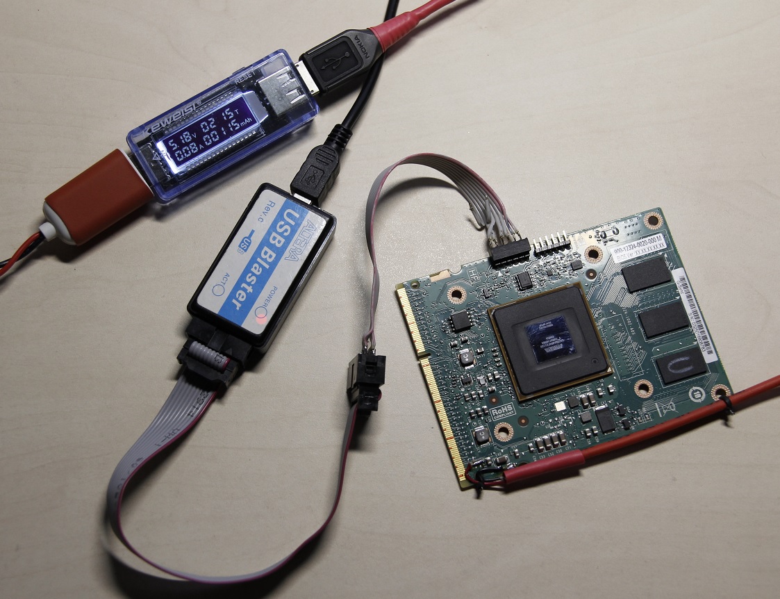
With Quartus Programmer it is important to delete the configuration stored in flash memory. If you carefully read the documentation on the Intel Arria V GX , you may notice that the BSDL file contains information, that is relevant only for the unconfigured FPGA chip. The warning is given at the beginning and end of the BSDL file .
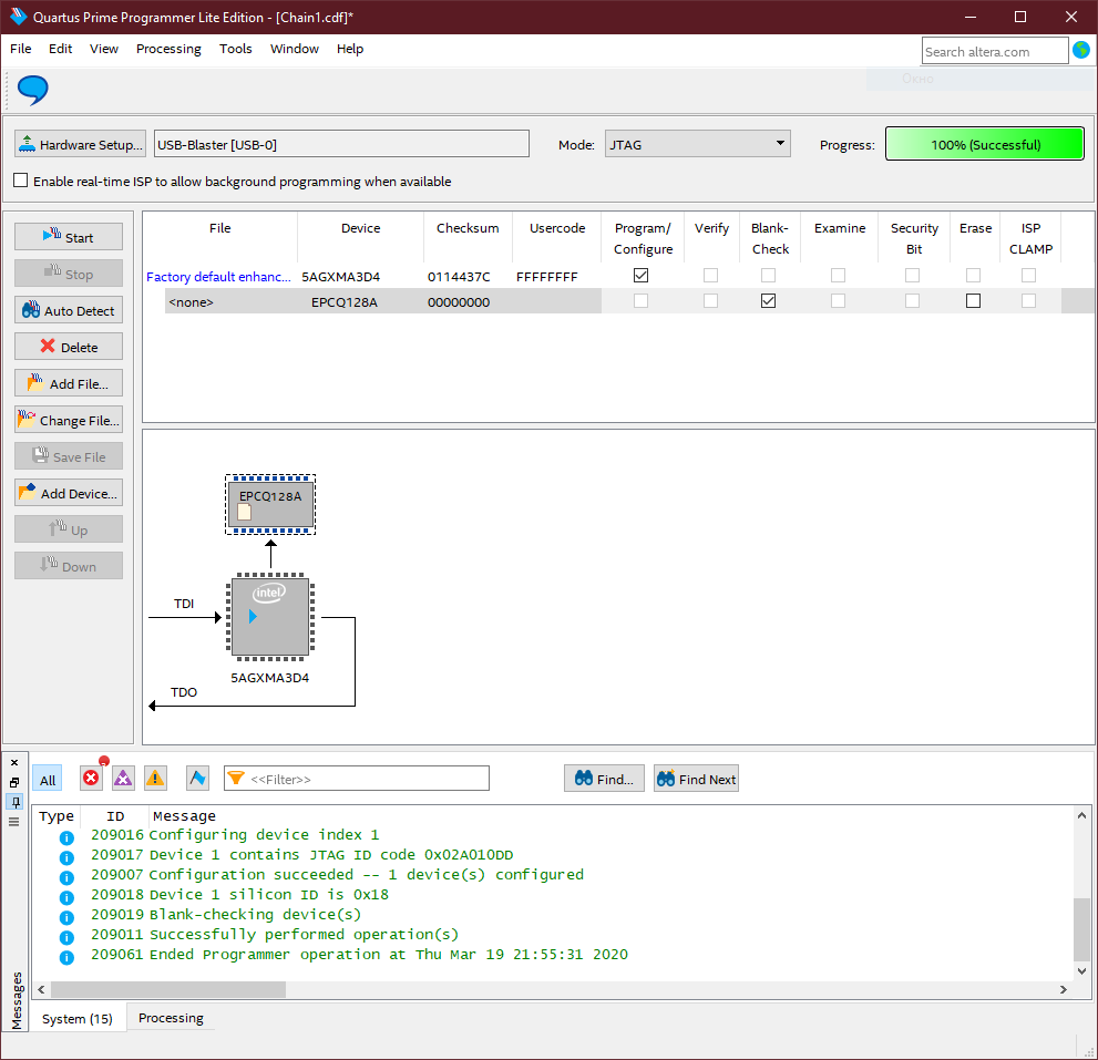
Once again make sure that the flash memory is clean, that so the FPGA will remain unconfigured after the board starts.
Step 3
Find the BSDL file for the Altera Arria V GX chip, in order to know following information:
attribute INSTRUCTION_LENGTH of ARRIA_V_5AGXMA3DF31 : entity is 10;
attribute BOUNDARY_LENGTH of ARRIA_V_5AGXMA3DF31 : entity is 1488;
...
"SAMPLE (0000000101), "&
This info can be added directly to the Arduino Code of the Device or entered manually while using the Device with the command "s" - Set SAMPLE Code.
Step 4
As you can see on photos below Serial USB Terminal for Android is used, though you can use any Serial Terminal, such as PuTTY for Windows/macOS. The Arduino board is connected to the phone with an OTG cable, the speed is given here .
When everything is connected properly, the command "i" - Info will give us some basic information about the chips connected to the JTAG Chain and display them on the terminal. Check carefully that the received information matches expectations.
Step 5
At this point, you can try monitoring mode by entering the command "m" - Monitor
The terminal will show numbers of bits that change in the Boundary scan register. These can be bits that reflect the state of real chip pins, as well as bits of some internal states. It is almost impossible to work with such a flow of information, so it is necessary to block displaying of bits that change without externally affecting the board. This can be done with entering the lock mode using the command "b" - Block.

After a while, new lines will stop appearing on the screen, this usually takes from 5 to 20 seconds. Then we can see the bit numbers that have been added to the lock register by typing "l" - List in the terminal.

As a result, we have a list of over twenty Boundary scan register bits that are constantly changing. This list of bits can be divided into two groups. First one contain bits, in our case, it is 0, 2, 9, 12, 13, 14, 15, 17, 21, 22, for which the only information, that can be found in the BSDL file is this:
  "0     (BC_4, *, internal, X)," &
  "2     (BC_4, *, internal, X)," &
  "9     (BC_4, *, internal, X)," &
  "12    (BC_4, *, internal, X)," &
  "13    (BC_4, *, internal, 1)," &
  "14    (BC_4, *, internal, X)," &
  "15    (BC_4, *, internal, X)," &
  "17    (BC_4, *, internal, X)," &
  "21    (BC_4, *, internal, X)," &
  "22    (BC_4, *, internal, 1)," &
Another includes the following bits 591, 627, 639, 642, 651, 663, 675, 687, 699, 714, 735, 747, 777 for which FPGA external pins were found.
  --BSC group 197 for I/O pin H6
  "591   (BC_1, IOH6, input, X)," &
  "592   (BC_1, *, control, 1)," &
  "593   (BC_1, IOH6, output3, X, 592, 1, Z)," &
  ...
  "627   (BC_1, IOF4, input, X)," &
  "639   (BC_1, IOM7, input, X)," &
  "642   (BC_1, IOL6, input, X)," &
  "651   (BC_1, IOJ4, input, X)," &
  "663   (BC_1, IOM6, input, X)," &
  "675   (BC_1, IOJ3, input, X)," &
  "687   (BC_1, ION8, input, X)," &
  "699   (BC_1, IOL4, input, X)," &
  "714   (BC_1, ION9, input, X)," &
  "735   (BC_1, IOR10, input, X)," &
  "747   (BC_1, IOP4, input, X)," &
  "777   (BC_1, IOT4, input, X)," &
Looking in the BSDL file, we can match the bits we received and external pins, as H6, F4, M7, L6, J4, M6, J3, N8, L4, N9, R10, P4, T4. These can be either clock pins or pins, that is connected to microcontroller MSP430G2553 on the board.
Step 6
This is the final step, where the main goal is to go through all the pins on the board, in order to find a matching pin of FPGA. Entering monitor mode with command "m" and connecting a special probe pin to external one gives us information about bits on the terminal, which we find in the BSDL file and write down information about pin.

The information that was found for 1170:
--BSC group 390 for I/O pin AB18
  "1170  (BC_1, IOAB18, input, X)," &
  "1171  (BC_1, *, control, 1)," &
  "1172  (BC_1, IOAB18, output3, X, 1171, 1, Z)," &
After a few hours this process is finally over and as a result we get the file with pinout .
Discussions
Become a Hackaday.io Member
Create an account to leave a comment. Already have an account? Log In.