Stephen Holdaway
-
Ticking accurately with the NEO-6M
08/07/2021 at 01:11 • 1 commentLike any normal person, I want a desk clock that has sub-millisecond accuracy.
Parsing and immediately displaying time from NMEA messages as they arrive from the GPS module, like GPS Wall Clock originally did, gives a useable-enough value for display, but it's not particularly accurate for a few reasons:
- The GPS module outputs messages at 1Hz, but each of these serial transmissions only begins once the GPS has finished its internal fix calculations. Fix calculations take a variable amount of time depending on the number of satellites being used in the calculation, which can be from 40 to 100ms for 1-12 satellites.
- At the default 9600 baud, a NMEA RMC sentence containing the current time will take 42 - 82ms to receive, depending on the number of fields filled.
- Converting the received time into segment data and sending to the MAX7219/MAX7221 over SPI takes some processing time.
To avoid these delays and uncertainties, the GPS module offers a
TIMEPULSEpin that can be used to generate interrupts on our controller at the top of each second with considerable accuracy.
Even with a good GPS signal, there's a significant delay between the tick of each second and the serial data containing that time. How accurate are we talking?
The u-blox documentation claims it's possible to get timing accuracy in the order of nanoseconds with ideal conditions, while accuracy in the order of microseconds is quite achievable:
As a rule of thumb the position should be known with an accuracy of better than 1m for a timing accuracy in the order of nanoseconds. If an accuracy is required only in the order of microseconds, a position accuracy of roughly 300m is sufficient.
Let's not get too carried away though - we're making a display for humans after all, where perception seems to take in the order of tens of milliseconds at best. In practice it will take someone much longer to look at and interpret the display.
Consider that in your day-to-day life, knowing the time to ±1 minute would likely be inconsequential, and ±1 second would be practically imperceptible. I would hazard a guess that the standard deviation of maintained time-keeping devices you encounter is at least 30 seconds, though I can't find anyone who has sampled this, and networked clocks probably tighten this guess up a bit.
I'm happy drawing a line at ±1ms, mainly because digging any deeper yields more and more uncertainty:
- What is the precision of the timepulse signal? (Something like ±30ns if the jitter and quantization in the module's 48MHz clock isn't compensated for)
- How quickly does segment data sent to the MAX7221 actually change the output signal? (The datasheet lists a maximum output propagation delay of 25ns)
- How fast do the LED segments actually light up? (It depends, but probably <1μS)
- How long does it take for light to travel from the display to your eyes? (about 3.3ns, if you're 1 metre away).
- ...ad nauseam ...
Given that I'm using these modules indoors and don't have equipment to verify absolute accuracy anyway, all of this is essentially academic, but it's fun to consider.
Using timepulse (1PPS)
The
TIMEPULSEpin on the GPS module generates a rising edge at the top of each second, with a configurable offset in nanoseconds to account for electrical and processing delays. Messages sent by the module always correspond to the previous timepulse, though the documentation only mentions this a few times briefly: vs serial data out (from the Receiver Description and Protocol Specification PDF)")
Order of the timepulse and serial data output (u-blox 6 Receiver Description, p27) To display the time correctly, we'll need to calculate the next time to display when a NMEA "Recommended Minimum" (RMC) message arrives. At the following rising
TIMEPULSEedge, this calculated time needs to be displayed. The MAX72xx will immediately update its display when any digit data is written, so the most I can prepare in my case is internally buffering segment data ready for blasting out over SPI.Due to the reversed wiring of the MAX72xx for common-anode digits on this project, all 8 "digit" registers always need to be written when updating any of the VQB-71 digits, even if only one digit has changed. This might seem like a disadvantage in terms of speed, but a consistent update time is actually better here as it can be compensated away using the module's user configurable timepulse delay setting.
A quick measurement of the delay between timepulse and a complete display update using a logic analyser gives a consistent value of 40.875μS (sampled at 200MHz):

Configuring this on the GPS module requires sending a UBX protocol command - specifically CFG-TP5. The UBX protocol is binary, but it's well documented by u-blox and doesn't take much code to send commands. The data for my timepulse configuration command looks like this:

Note that timepulse is only guaranteed to be aligned with the top of each second if "GPS time is locked". As far as I can tell, a lock on GPS time doesn't necessarily require a position fix, but it does require the receiver to have a decent quality signal. NEO-6M modules in their default configuration won't output the timepulse signal unless GPS time is locked, but this can be tweaked using the
CFG-TP5UBX command, as I've done here.If you don't want to write any code, these GPS modules can be connected to a computer by UART and configured using the u-center tool (Windows only) from u-blox.
Further reading
As mentioned, the official documentation for these modules is very good:
- u-blox 6 GPS modules datasheet (NEO-6)
- u-blox 6 Receiver Description including UBX and NMEA protocol specifications
- GPS-based timing considerations with u-blox 6 GPS receivers (app note)
- NEO-6 hardware integration manual
Since writing this article, I've also applied the same timepulse upgrade to the ATTiny-based wall clock - surprisingly managed to make it fit!
-
Design and bring-up of a VQB 71 GPS clock
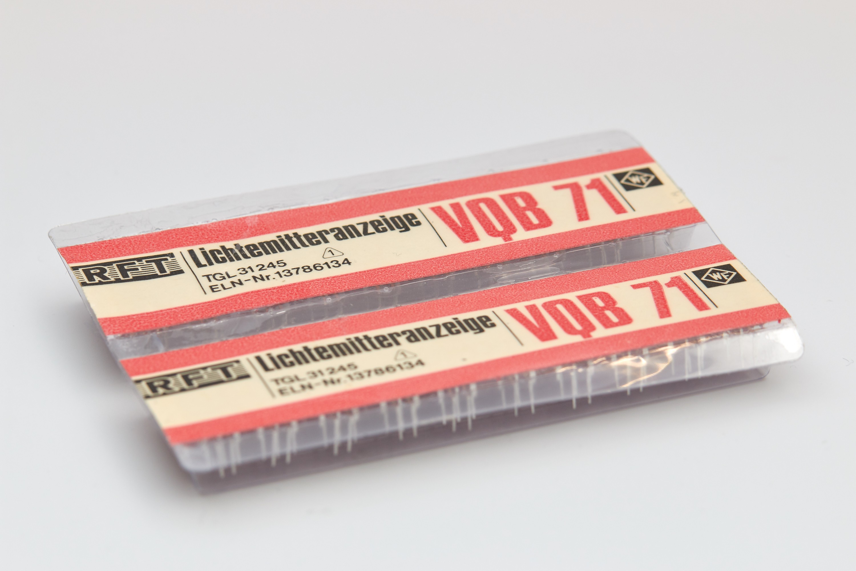
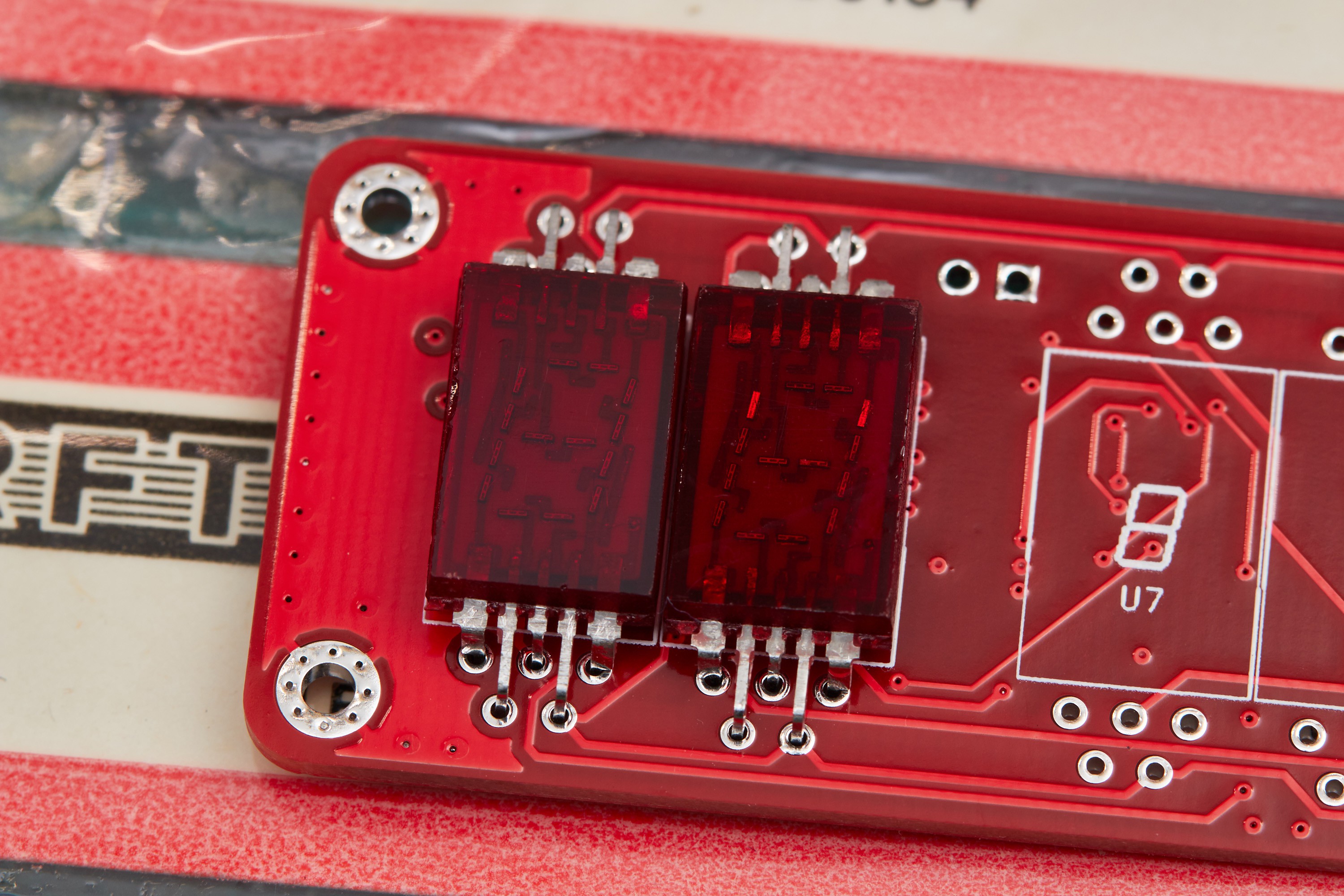
03/29/2020 at 05:15 • 2 commentsA year ago I picked up some new-old-stock "VQB 71" 7-segment displays — not for any particular project, but simply because they looked fantastic. These gorgeous, vintage common-anode digits have distinctive segments with six tiny LEDs each, internally connected with bond-wires and encapsulated in transparent red epoxy/resin:

Microscope photo of an unpowered VQB 71, lit to reveal its internal features. Hundreds of tiny bubbles can be seen in the red epoxy under this lighting, which aren't visible to the naked eye. The digit height within the display is 7mm. This batch was manufactured in 1989* by WF Berlin (Werk für Fernsehelektronik), a division of the East German state-owned company VEB Kombinat Mikroelektronik Erfurt. The packaging is titled "lichtemitteranzeige" which is literally "light emitting display": an odd name by modern standards according to a German colleague of mine, who said this would simply be labelled "sieben segmentanzeige" today.
![Tray of 20 RFT Lichtemitteranzeige VQB 71 7-segment LED displays made by WF Berlin in June 1989]()
![VQB 71 displays in packaging]()
* The marking "X06" indicates a manufacture date of June 1989, assuming Wikipedia is correct about the manufacturer using IEC 60062 letter and digit codes. WF Berlin appears to have phased out most of its manufacturing in 1990 (source), so a mid-1989 date makes sense for new-old-stock parts. A few partial scans of datasheets for the VQB 71 are available online, with the one below from tu-chemnitz.de being the most complete copy I've found. A datasheet isn't strictly necessary here, but it's useful to have dimensions provided for the footprint, and I wanted to know the maximum current per segment specified by the manufacturer. After all, These parts haven't been made for nearly 30 years, so it would be a shame to destroy one accidentally.

VQB 71 datasheet scan. The contents of this image is transcribed below. It's easy enough to figure out the specs without knowing any German, but Google Translate makes quick work of the dry/technical language. Here's the English translation of this datasheet:
VQB 71
Not for new designs
Light emitting display made of red-beam GaAsP diodes in a segment design to display the digits 0...9 and a decimal point (DP). The wavelength of their max emission is 630...690 nm. The half width is 40 nm.
Limits Forward direct current / segment or DP at θa -25...25 °C IF max 15 mA DC blocking voltage at θa -25...+70 °C UR max 4 V Operating temperature θa -25...+70 °C Storage temperature for storage up to 30 days θstg -50...+70 °C Characteristic values at θa = 25°C Luminous intensity / segment at IF = 10 mA IV typ 150 μcd ↳ Decimal point IV typ 100 μcd Forward DC voltage / segment at IF = 10 mA UF max 3.6 V ↳ Decimal point UF max 1.8 V Note that unlike modern LED datasheets, this doesn't specify maximum pulsed currents. Pulsed currents with modern LEDs are typically 3-5x the max constant current rating (dependent on duty cycle and pulse duration), which can give some head-room for driving them harder in multiplexed configurations.
Driving these segments with a constant 10mA as the datasheet suggests gives a high-contrast image in vivid red. The VQB 71's are so intensely red that it's proved difficult to capture an accurate representation of one on camera. Modern LEDs like those in the GPS Wall Clock look almost orange by comparison.

Segment powered with a constant 10mA source. Note that the segment is completely over-exposed here. With no light cast on anything, it's difficult to convey the true brightness. 
Same as above, but exposed for the segment - a reduction of 7 whole stops. Driving all segments at this power increases the surface temperature of the digit by around 10°C, but who needs efficiency when you have style, right?
I hear we're building another clock
There are only so many applications for a 7-segment display these days, and I'm a firm believer that one person can never have enough clocks. A miniature version of the GPS Wall Clock for a desk seemed like a nice way to put these vintage digits on display.
This time around there are a few changes:
Bigger processor
It was fun squeezing the original implementation into 1KB of code space on an intentionally small part. This time I'm more interested in expanding functionality: better display accuracy, configuration of the GPS module, more buttons, less pin-sharing, etc. Initially I'd picked the ATMega88PA as I already have a tray of them, but after a first pass on the schematic it was obvious most of the pins would go to waste. I traded it for the physically smaller but otherwise comparable 8-bit STM8S003F3P6.
Due to a shipping error a few years ago, I have more than 100 of these STM8S chips, so they're an easy choice. While not necessarily a popular chip, these are half the price of similar AVR chips new, can be programmed with the dirt-cheap STLinkV2 dongles available from the usual suspects using a SWIM interface, and can be used with an open-source toolchain. The downside is that it's just you and the reference manual when things aren't working, but hey, I enjoy that challenge.
![]()
The die of an STM8F003F3P6 (2.35mm wide), sitting on a VQB 71. Decapped semi-successfully without chemicals using the method in this video from CuriousMarc GPS module on-board
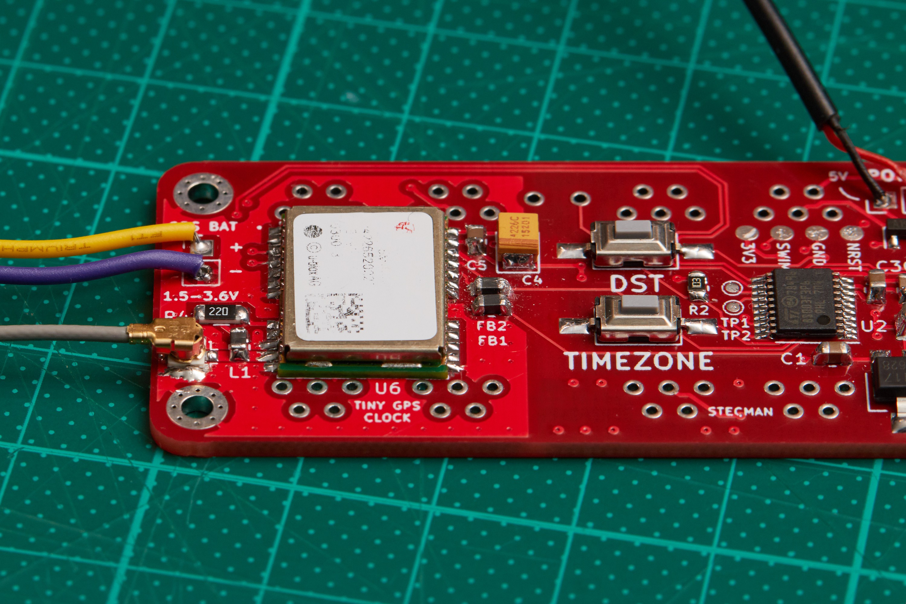
Like the original, a GPS receiver will provide time information *from space*, but this time the GPS module will be integrated into the layout instead of wiring up a separate breakout board. New GPS modules from distributors start at about $15 NZD each, so I went the cheap way and grabbed some grey-market u-blox NEO-6M modules for about $5 NZD each. The units I received appear to be leftovers from a production run that have been sitting in a factory for years collecting dust, but they do work correctly.

Seemingly legit and unused NEO-6M modules, with bonus corrosion and dust. These work fine, though I don't want to know where they've been sitting for the 5+ years between their 2013 manufacture and me buying them in 2019.... Improved accuracy
The GPS module has a
TIMEPULSEpin that generates a rising edge at the top of each second by default. I was aware of this in the original project, but didn't have any spare pins or program space to handle it. The original build updates its display each time a NMEA RMC ("Recommended Minimum") sentence is received over UART, which works fine, but does make the clock run almost a tenth of a second slow:
This is already accurate enough for practical human purposes, but we can go deeper. Offsets can be configured in the GPS module to account for electrical and processing delays, so in theory it's possible to have nanosecond accuracy. Since this is only keeping time for humans, I'd be very happy with ±1ms accuracy.
Schematic and layout

In the spirit of vintage parts, I've printed and scanned the new schematic several times to enhance its character. (Click for the original colour schematic). Only a few things of note here:
- The MAX7219/MAX7221 is designed for common-cathode segment displays, but the VQB 71 is common-anode. Wiring the display "backwards" with segments to digit pins and digits to segment pins allows this to work. The trade-off is needing extra software to handle the memory layout being oriented around segments instead of digits:

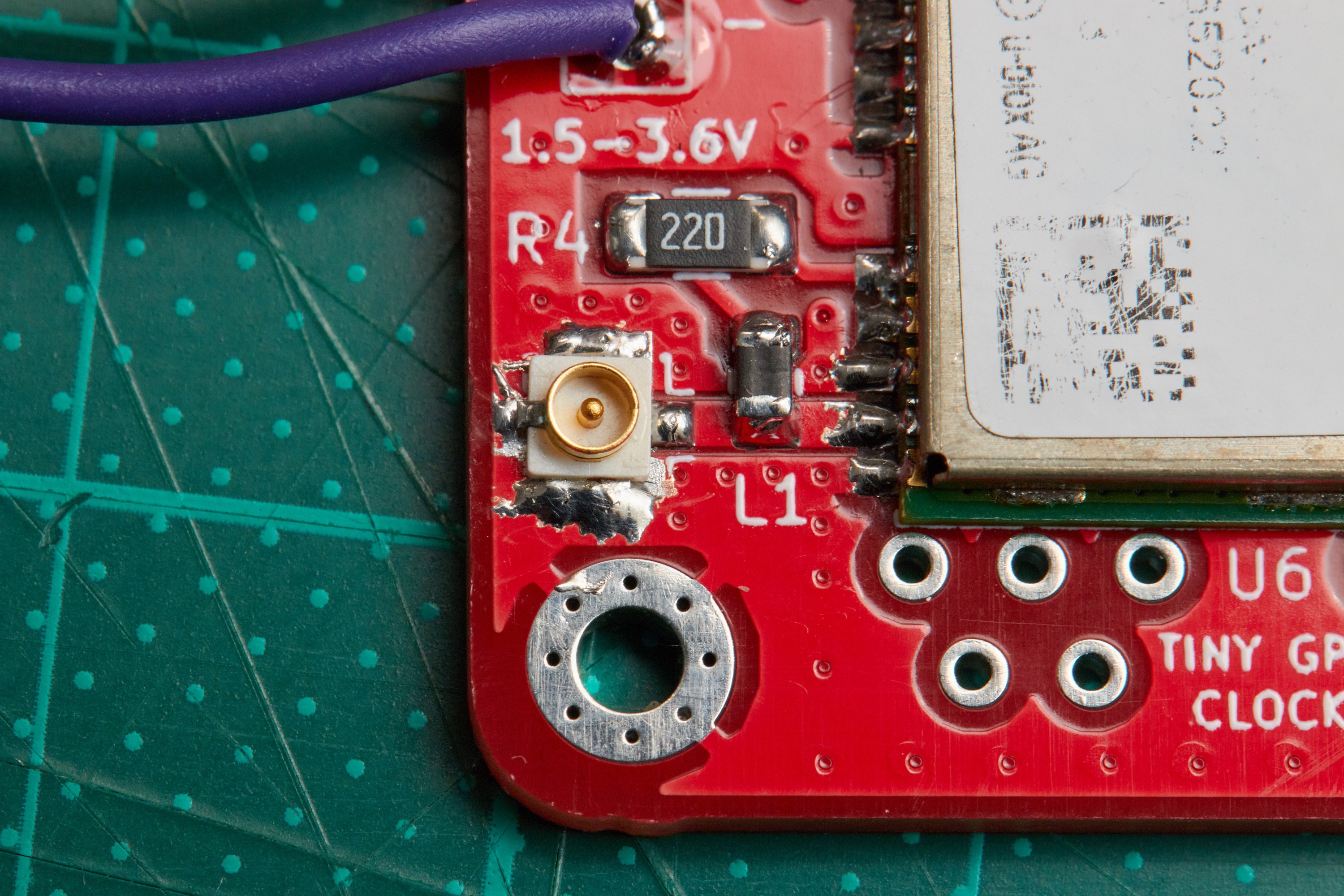
- The NEO-6M uses the active antenna configuration from u-blox's Hardware Integration Manual. The module technically doesn't need anything else to function, but I've attached the backup battery to avoid cold starts when briefly removing power, since those are painfully slow and require good reception. This is intended to be powered 24/7, so there's no need for an external flash/eeprom.
- The power input is 5V with simple polarity protection, regulated to 3.3V for the GPS module and the STM8. This will probably be wired to USB once it's in a case.
- Similar interrupt sources are grouped by port to make interrupt handling simpler. The STM8S lacks dedicated pin-specific interrupts like AVRs tend to have (INT0, INT1, etc) and instead has a shared interrupt per port for pin changes.
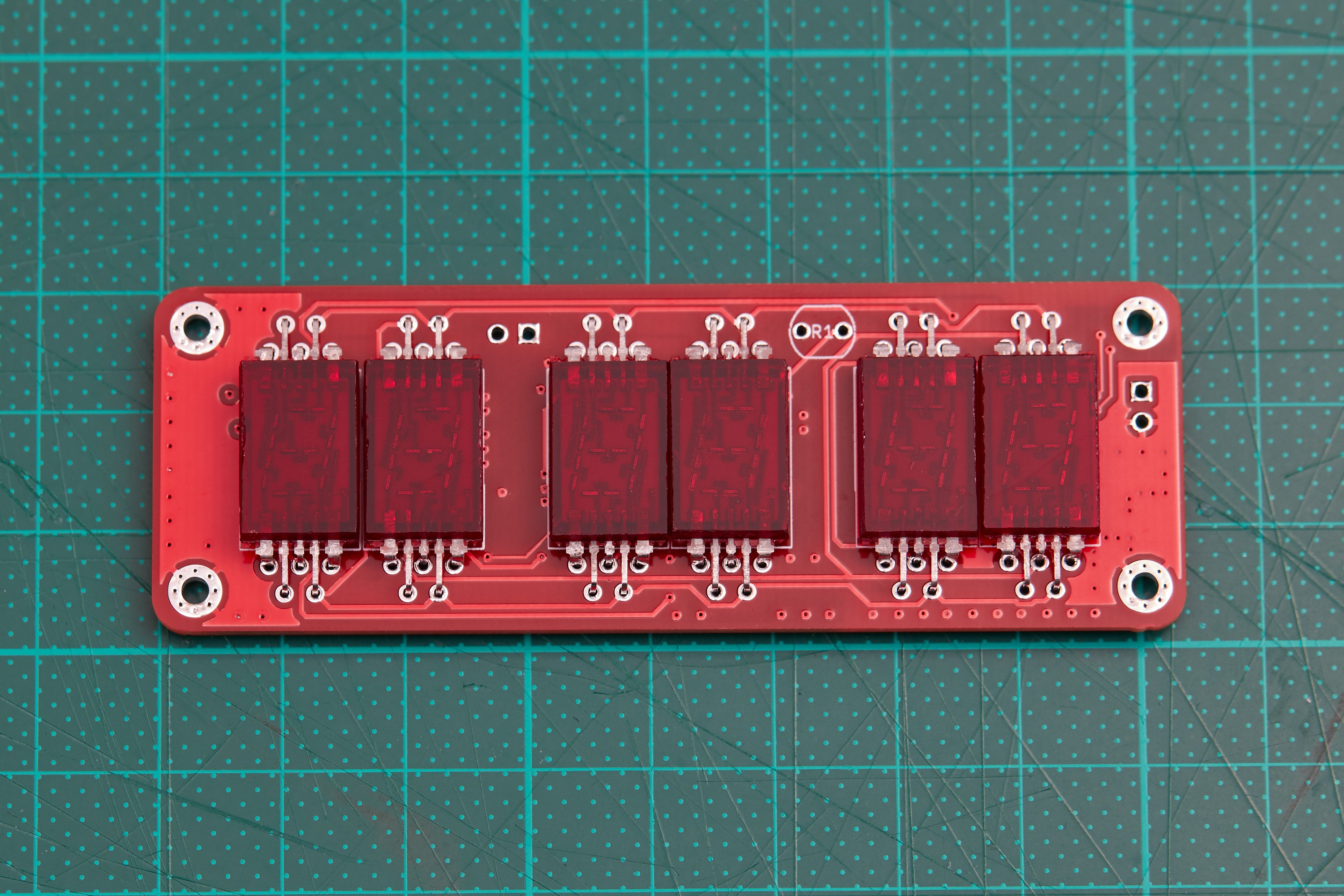
This project started as a two-layer board just big enough for six VQB 71 digits, but it quickly became apparent that I was either going to need to make the board larger or go to four layers. I went with the latter as it wasn't prohibitively expensive to jump from two to four layers. It's possible this could've been routed with two layers, but I suspect it would've been quite time consuming. Space around the GPS module is particularly tight, but almost everything I wanted fit:

I'd originally tried to fit a CR2032 battery holder into the layout, but that was taking up 30% of the back and was cut in the end. To save space, the battery is exposed as a header and will reside in the eventual enclosure. The top layer is likely going to double as a front-panel, so I avoided using the space for general layout.
While the circuit is relatively straight forward and uses parts I've worked with before, the GPS module was something I wanted to be extra careful with. I've done zero RF work before, but the NEO-6M's hardware integration manual provides plenty of guidance around antenna layout. This manual in combination with study of existing NEO-6M breakout boards gave me a small amount of confidence that this wouldn't be a reception disaster. The digit pins being so close to the GPS module is an unknown, but there's not a lot that can be done without making the board a few centimetres longer (something I played with early on, but didn't like the look of).
The board went to fab mid-February, was manufactured over the course of 10 days, and took a further 10 days to get to my bench in New Zealand. I went with red solder mask to match the digit casings. It's still hard to beat fresh, shiny new PCBs:

Assembly in pictures
![]()
A little fiddly to align all of the digit pins, but they fit well. I'd previously test fitted digits on a print-out of the layout, but it's nice to see the spacing work on the real board. ![]()
All aboard (still test-fitting) ![]()
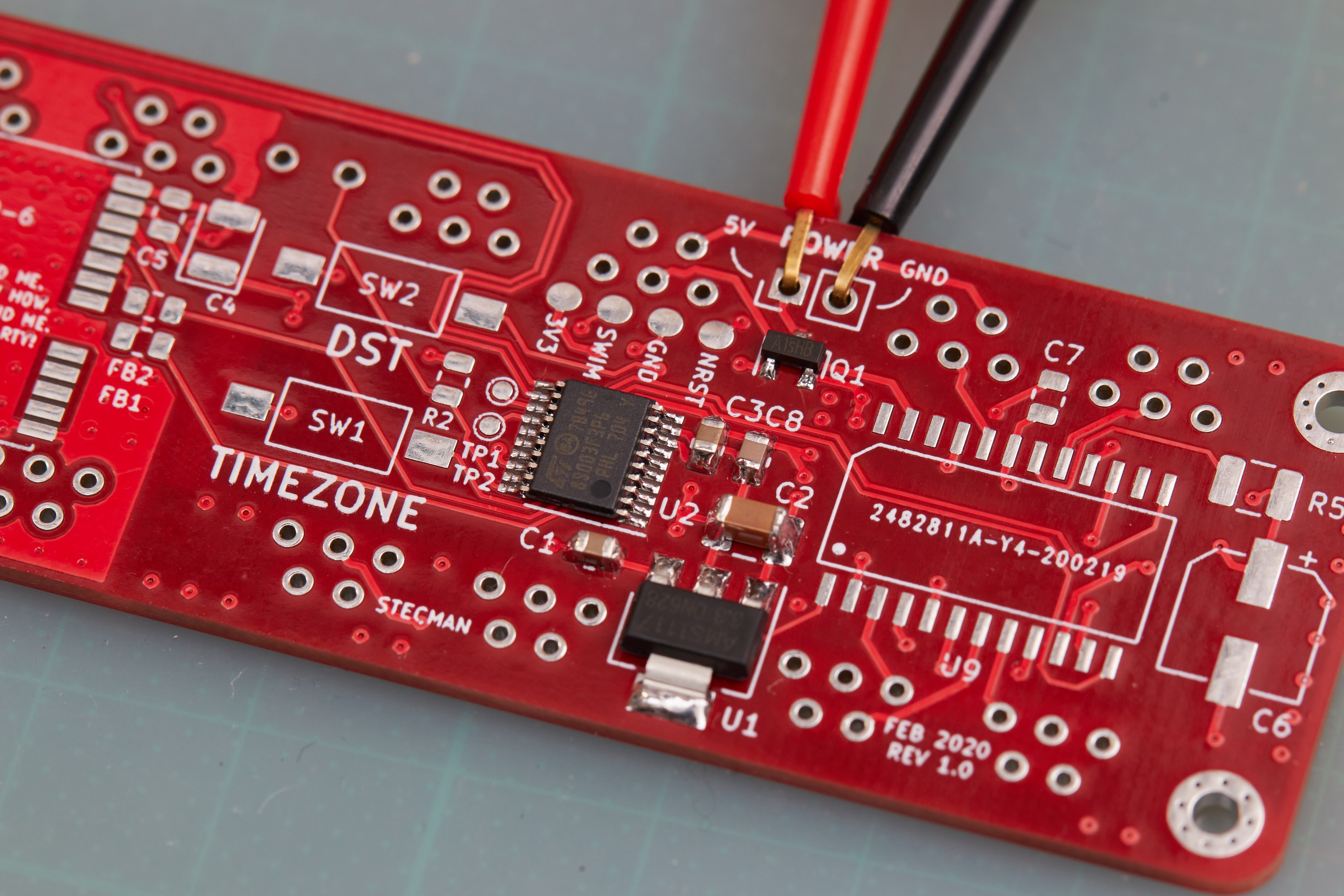
3.3V regulation and the STM8 microcontroller soldered and tested. The polarity protection MOSFET ended up saving me later when wiring a cheap USB cable that has black-positive and red-negative wires! ![]()
Things didn't go quite as cleanly getting the NEO-6M module installed. I went through a couple of I-PEX connectors getting my iron temperature right for working on the large ground plane around the GPS module. I also found that the module's sticker had almost no resistance to the isopropyl alcohol I use to clean off flux. ![]()
Close-up of the damaged solder mask where reworking ground connections was challenging. 
Fully assembled board. The MAX7221 chip went on and was tested before the GPS module, but I forgot to take photos of that. Firmware
To get the clock up and running quickly, I ported the code from the original AVR project to run on the STM8. This only required swapping out a few registers and pin mappings, replacing the SPI, UART and ADC implementations, and adding mapping to set BCD values on the common-anode wiring of the MAX72XX.
When I went to display actual data on the display and turned off the driver's test pattern, I discovered I'd wired the digits in the order {0, 4, 3, 1, 5, 2} instead of the expected {0, 1, 2, 3, 4, 5}. I'd tested with a MAX7219 to find the correct output for digit 0, but I either didn't test the other digits or the MAX7221 has a different output order to the MAX7219. This was a simple fix in software anyway, adding to the existing mapping code.
I'll work more on the firmware over the next few weeks, but for now there's a working clock:


- The MAX7219/MAX7221 is designed for common-cathode segment displays, but the VQB 71 is common-anode. Wiring the display "backwards" with segments to digit pins and digits to segment pins allows this to work. The trade-off is needing extra software to handle the memory layout being oriented around segments instead of digits:

 vs serial data out (from the Receiver Description and Protocol Specification PDF)")