When you design a circuit with fast digital buses, sooner or later you come to the point to worry about setup and hold time and the timing skew between the bus signals. Hopefully, your manufacturer provides you some guidelines about the maximum allowed timing skew between certain (groups of) signals. In my case, Cypress has a nice appnote for the hyperram devices. A big "thumbs up" at this point!
")
By looking at the table, it is easy to imagine that a) manually keeping track of different length matching requirements is error-prone and b) using the toughest requirement for all is not an option. How does KiCad help me with length matching? - Well, it has a nice interactive assistant that helps me adjust the length of one trace (or one diff pair) to a specified value. However, there are a few inconveniences here:
- How do I specify and save the allowed tolerances for each line in the tool?
- How can I see which requirements are fine and where tuning is still needed?
- Actually, KiCad wants to know about a length, but I only care about a relative length tolerance (as long as it is not insanely long)!
- My FPGA has no matched 50Ω output drivers, so I would like to use a series termination scheme. Therefore, the connection from the FPGA to the hyperram gets split into two separate nets. I really don't want to measure and match lengths on 24 individual nets per ram chip!
- Vias are not considered.
The good news, other people had the same problem and came up with ideas! There is a kicad-length-matching-checks script and a modified version by the never resting Greg Davill, but I only found that one later and have not looked into it. To more or less solve all four points listed above, I tried to hack together my own version, loosely based the first script.
I quite dislike the idea of creating weirdly named net classes (it is also not flexible enough), so I took on an idea Chis Gammel once discussed on TAH. He suggested to put text boxes with additional descriptions and calculations on your KiCad schematic, but outside of the nice printing border. If you generate a pdf version the clutter will be excluded, nevertheless it is easily accessible and less likely to get lost. As a result, I have little text boxes to define all tolerance requirements:
LENGTH MATCHING:
id: hyperram1_dq
netnames: "(?:/hyperram/)?HR1_DQ[A-Za-z0-9_-]+"
merge: "^(?:/hyperram/)?(.*?)(?:_R)?$"
tolerance: 1.27 mm
vialength: 1.6 mm
ID is just the name of this rule definition block, which will be shown in the length matching report later. To define which nets should be considered by the rule, you simply write down a regular expression for the NETNAMES parameter. All nets matching to this regex will then be piped through the MERGE regex. This step splits the net name into a base name and an optional extension and all equal base names will be treated as one big net. In my case, I have "HR1_DQ1" as net name between the FPGA and series termination resistor and then "HR1_DQ1_R" for the connection from the resistor to the hyperram chip. TOLERANCE is the maximum allowed length difference within all nets in this group and VIALENGTH defines how to account for vias. The overall length of the "DQ" lines is not restricted.
LENGTH MATCHING:
id: hyperram1_rwds_to_dq
netnames: "(?:/hyperram/)?HR1_RWDS_N[A-Za-z0-9_-]*"
merge: "^(?:/hyperram/)?(.*?)(?:_R)?$"
reflength: group hyperram1_dq
tolerance: 0.635 mm
vialength: 1.6 mm
The "RWDS" line must be closely matched to all "DQ" lines, which is expressed by the REFLENGTH parameter. Its arguments "group hyperram1_dq" tells the script to use a dynamic calculated length instead of a static (hard coded) one. Obviously the tolerance in the "hyperram1_dq" is dictated by the RWDS-to-DQ requirement, so it is basically overspecified. As long as you do not specify mutually exclusive rules, there will be no problem.
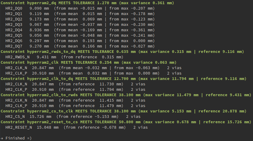
The basic workflow is stolen from the other script. You edit your layout while having the script running and as soon as you hit save, all your requirements found on a selected schematic page are tested against the pcb layout. At the end you hopefully get something like this:
 The script (work in progress) can be found on the project page: bus_aware_length_matching_verification.py
Happy hardware hacking!
Knusperkeks
Discussions
Become a Hackaday.io Member
Create an account to leave a comment. Already have an account? Log In.