 Michael Möller
I think I now have the right block diagram. The first one was easy, took 5 minute sketch, the SUBLEQ is sooo easy. Yeah - after thinking about it, there was an error here. Oh and an ommision here. And hey, indirect addressing on everything! "Rinse and Repeat" the design a few cycles.
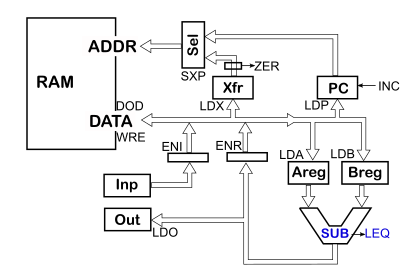
Note that input and output is included as an extension to the pure SUBLEQ. There is no other instruction than SUBLEQ, so INP and OUT are memorymapped, ie addressing location 0 will read INP (switches) or write OUT (7seg digit). Edit: It is not strictly memory mapped, as referencing address zero changes the way the instruction executes, rather than redirect the address.
XFR, Areg and Breg are latch-registers, PC is a presettable counter, SEL a 2-to-1 selector, SUB does subtraction and signals LEQ. The ZER senses address zero. ENI/ENR are tri-state gates (can't seem to design my way out of using tri-state on the databus, as it is bidrectional).
This of course needs some squencer to control, the microsequencer
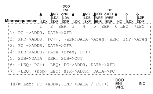
The last line is the Hardwired Loader - to be implemented as a push button that transfers INP to RAM, then increments PC.
Discussions
Become a Hackaday.io Member
Create an account to leave a comment. Already have an account? Log In.