 Michael Möller
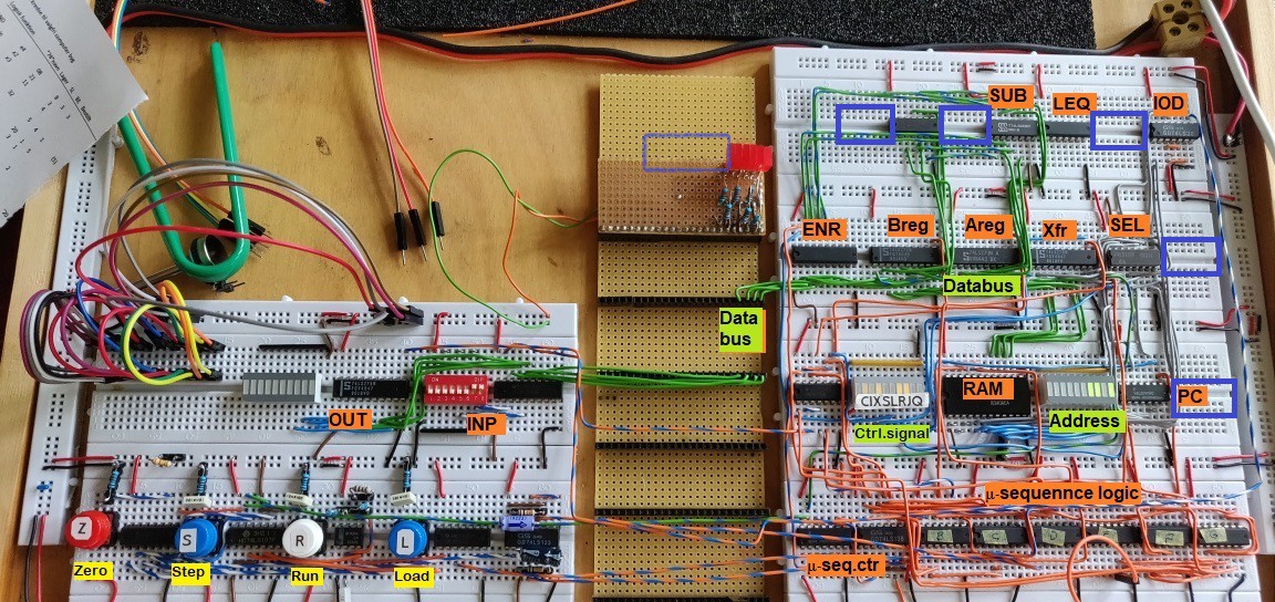
SUB (ALU)
The Full adder ('283) is placed in top row, plus an inverter for the Breg input, so it becomes a SUBtractor. The IOD (the I/O-detector, previously called ZER) signals on all-1's on the XFR-register output.
Placed, but not yet wired, is the LEQ detection on the SUB output.
Test
Of course, I had to test this interim stage, before having done the LEQ. I loaded 4, 5, -1, 5, 3 into the RAM, and then microstepped and verified that all the expected lights lit up. Thus it did one SUB(nobranch) instruction, and the correct numeric result. Yes ! Wave !
Onwards to wiring up the LEQ and then need to write tiny test programs. Thinking, "read INP and add it to running total on OUT". Oh, no conditional branch in that. Hmm... I only have room for 4 instructions and 3 variables
The Halt is not done, and I have to think how it should stop the clock.
8 bit ready
So far it is a 4 bit data/addr. There is room (in the blue boxes) for the chips One counter, one Adder, one inverster one OR gate) to make it 8bit as soon as the 4bit is working. The Bus-display needs widening, too. But before that, I'll do an Arduino "interface" so I can load RAM with program. Toggling in with the Load button gets tedious real quick.
μ-sequencer (3rd version)
Another "minor" rework of the controlsequence logic. I just stared hard at the logisim circuit long enough, tweak and simulated and found a way to free up 3 gates, even with the additional constraints included. I also managed to reduce the wiring mess, a little.
ToDo: include some logic to reset the sequencer in the non-branch case or indeed skip the 8th step as it is a 3bit counter.
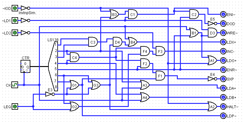
The A1 etc refer to chip/gate. (The inverters top left do not exist in the real circuit, only in the simulator, beacuse the signal is active low, so the Input buttons are easier to work with as active high.)
Discussions
Become a Hackaday.io Member
Create an account to leave a comment. Already have an account? Log In.