 James Wilson
With components selected, it's time to move toward realizing this converter. The next step will be testing the design in a circuit simulator.
People like to gripe about LTspice's outdated UI, but I've gotten pretty fast at sketching up circuits with it. Unfortunately, the LM5155 SPICE model is encrypted and only works in TI's SPICE variant, TINA-TI. TINA-TI is free to download and use, but LTspice is in many ways leagues better. Want to peek at some node voltage? In LTspice, just click on the node in the schematic after the simulation is done. In TINA-TI, the transient simulation only records voltages and currents for explicitly added meters, so that means adding a meter and re-running the simulation.
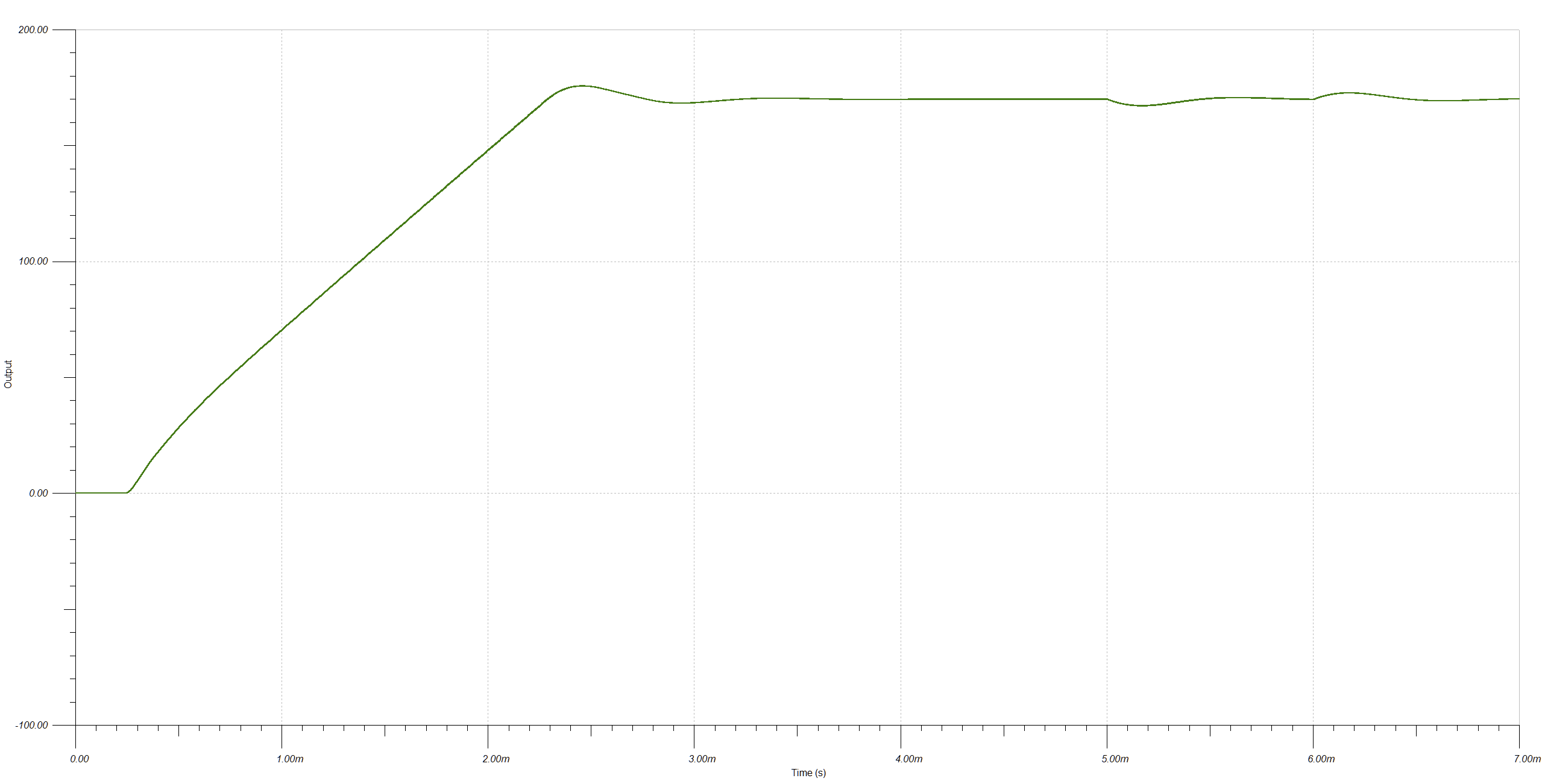
Here's the converter schematic in TINA-TI: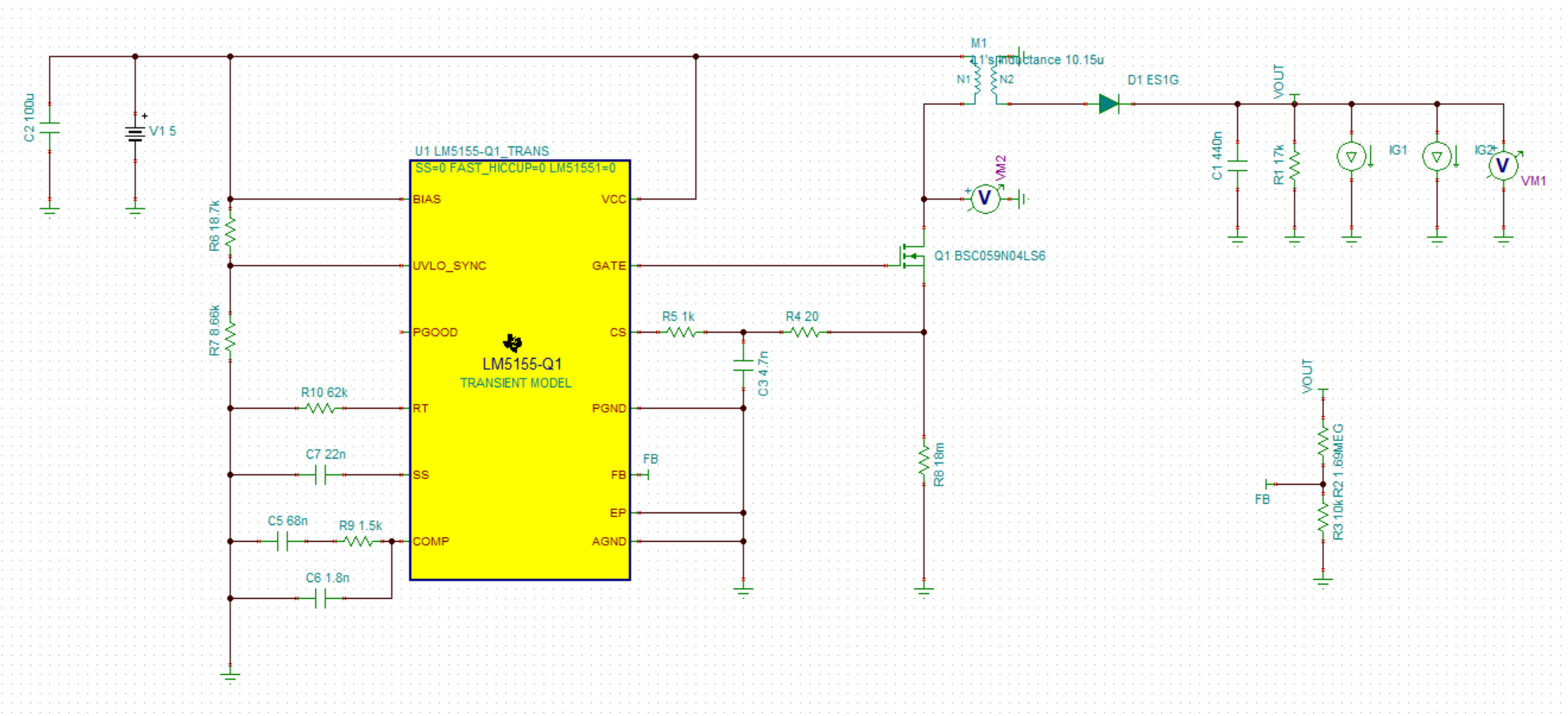 I changed the initial load to 11.33k to get a 15 mA output current and added time-delayed step current sources IG1 and IG2 to simulate a load step-up and step-down of 15 mA. Here's the output voltage plot, showing the startup ramp and load step at 5 ms/6 ms:
 Close-up of the load step transient shows the transient is larger than 1 V as predicted by formula used to pick the output capacitance, but it seems acceptable for the application. The converter returns to regulation within a millisecond and shows good stability.
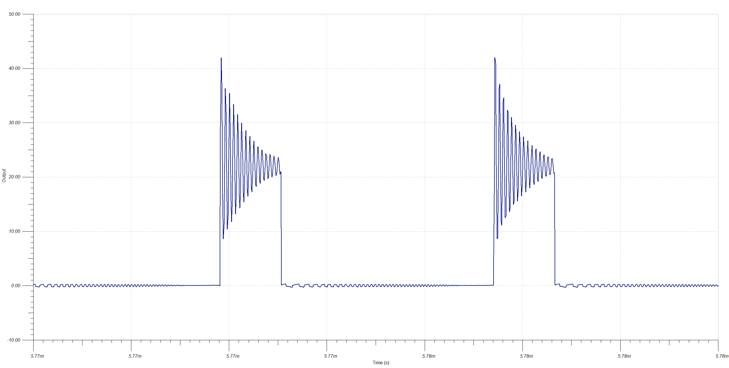
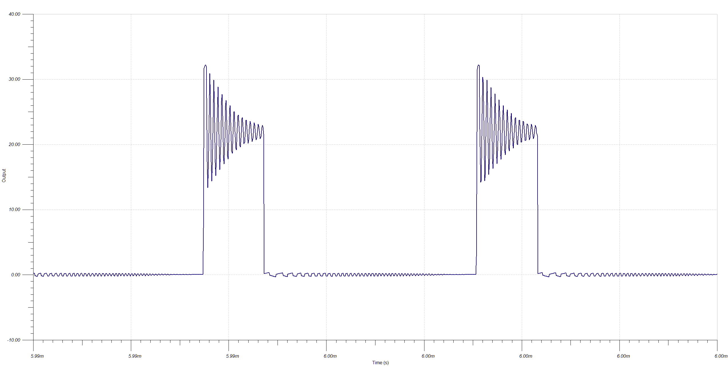
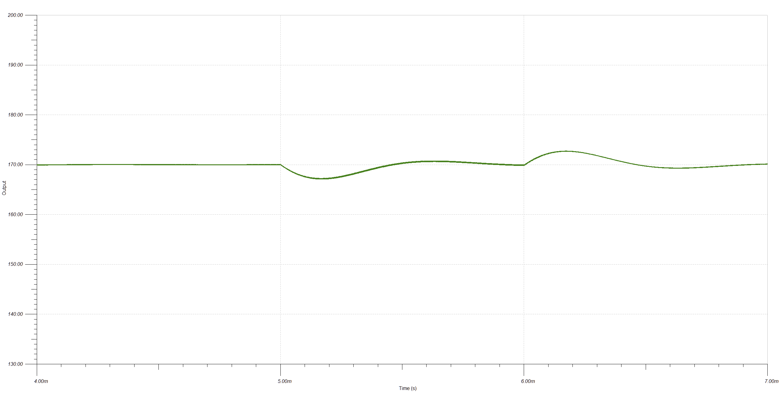 Looking at the switch node or MOSFET drain at full load, there's a problem: the voltage is spiking above 40 V and will need a snubber.
To build the snubber circuit, I turned to application note from Fairchild Semiconductor, AN 4147, that describes how to design a RCD snubber for a flyback converter. Even though it has "RC" in the name, the RCD snubber is nothing like a RC snubber that tries to damp resonance through matching the characteristic impedance of the parasitic elements. I spent a lot of time trying to understand this circuit before I realized it's actually similar to a boost converter that's driven by the resonance between the leakage inductance and MOSFET output capacitance, instead of a PWM gate driver, making it a kind of resonant converter! In this case, I selected a snubber voltage of 32 V or 80% of the MOSFET's rating, and the design equations in AN 4147 yielded R = 5.1 kΩ and C = 18 nF. I picked 1N4150 as the diode, it's rated to 50 or 75 V depending on the particular manufacturer, and is quite fast. This is the snubber circuit added in the simulation: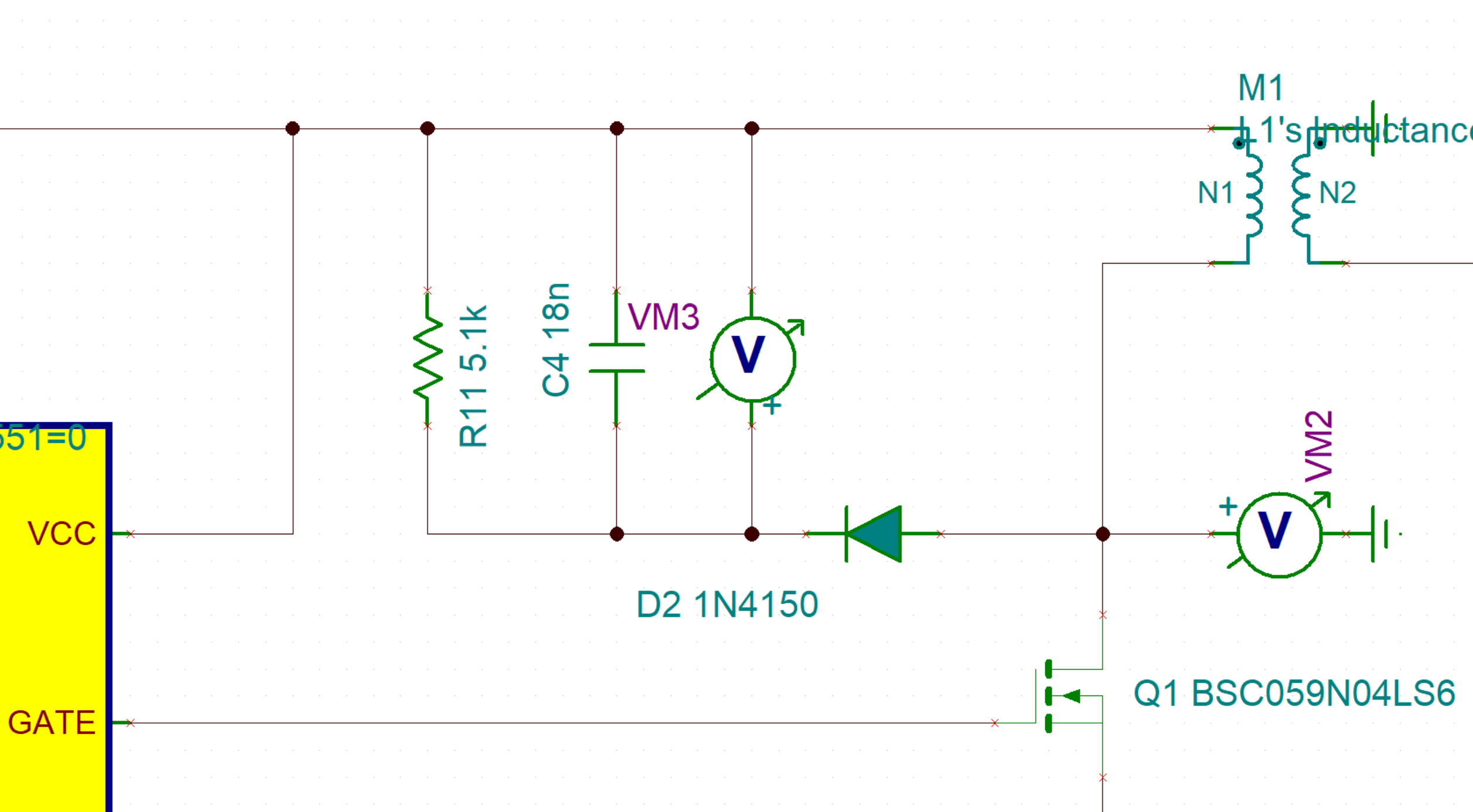 The simulation with this circuit added shows the switch node voltage gets clamped at 32 V as predicted. There's still a lot of ringing, but the goal of protecting the MOSFET has been achieved. Snubbers always need experimental verification and tuning, but this looks like a promising starting point.
Discussions
Become a Hackaday.io Member
Create an account to leave a comment. Already have an account? Log In.