 James Wilson
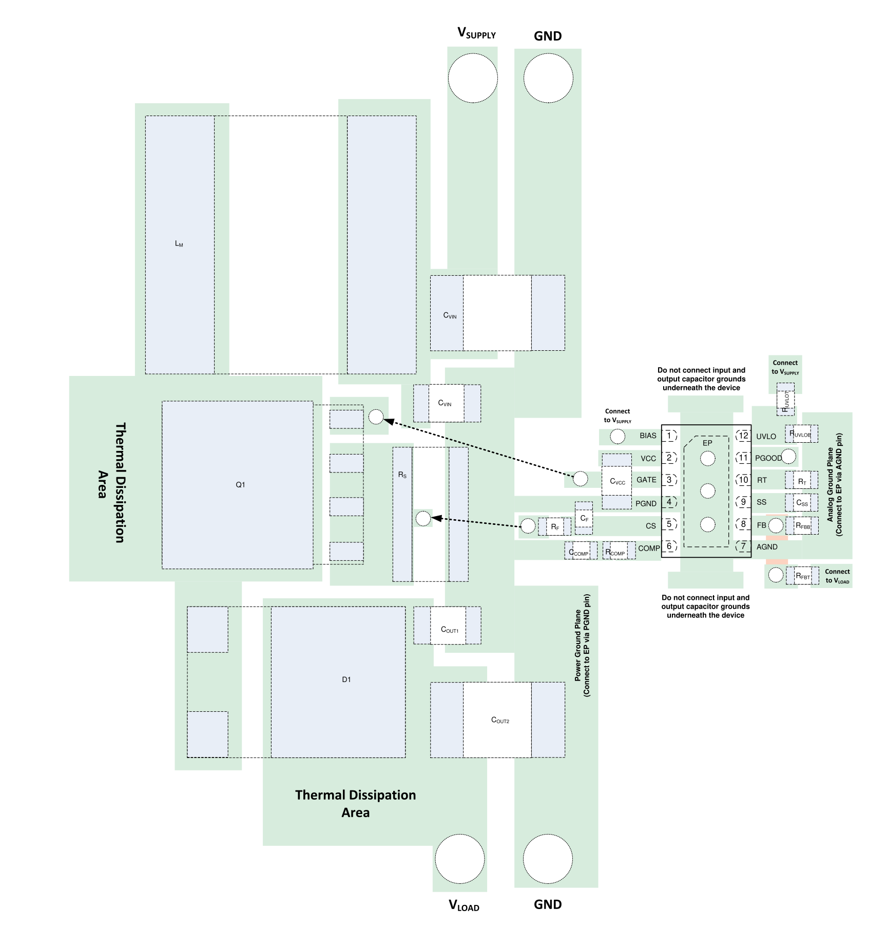
For this project, I wanted to justify all component values from first principles. On the other hand, for PCB layout of a SMPS, I'm more than happy to copy a layout that works. In this regard, the datasheet for the LM5155 provides very helpful layout guidelines and examples, and the engineering team at TI also produced three evaluation boards (in boost, isolated flyback, and SEPIC topologies) that also demonstrate good layout.
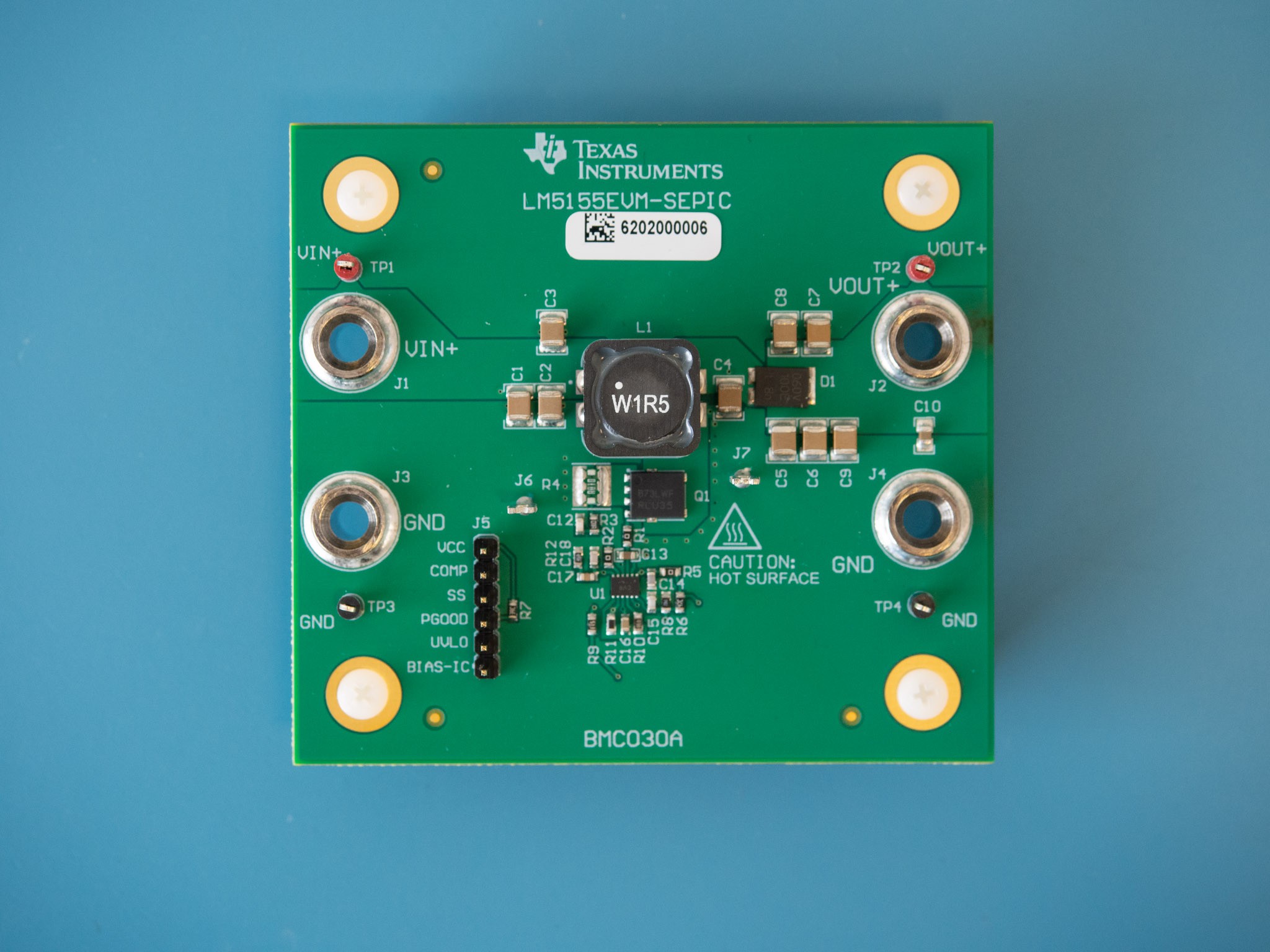
For my test board, I wanted to follow in the "evaluation board style", which to me means:
- Medium- to low-density design where there's plenty of room to probe and rework parts. Anything that I think I might tune, I use low-density footprints and leave space to rework the area and bodge on parts.
- Prefer larger component packages that are easier to rework, no smaller than 0603 for passives.
- Lots of test points. Commercial boards often use soldered-on loops for test points, but these get expensive in quantity, and an exposed pad with a nearby ground point works just as well.
- Power terminals accept big banana plugs for fast, positive connections to meters and power supplies.
- Screw holes and standoffs at the corners make it easy to keep the board stationary while attaching probes.
As the flyback power stage is the only thing on the board, routing should be uncomplicated, and I used a 2-layer layout like the examples and commerical evaluation boards.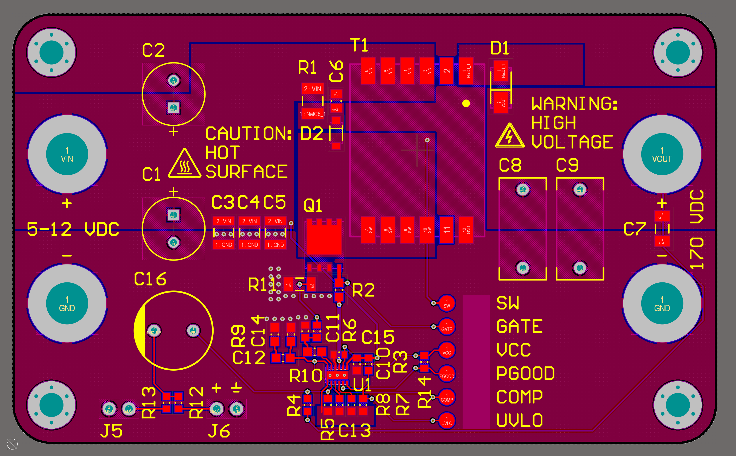
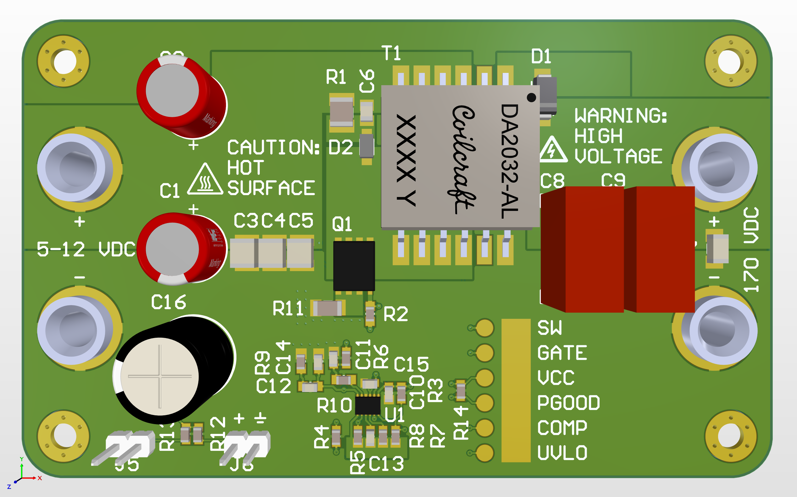 Next step: send for manufacturing, assemble & test!
Discussions
Become a Hackaday.io Member
Create an account to leave a comment. Already have an account? Log In.