 James Wilson
A converter needs a feedback mechanism to maintain voltage regulation. The choice of a duty cycle only works for a particular set of load resistance and input voltage. Variations, large and small, need to be corrected to maintain a stable output voltage level. Feedback loops are fickle things, and unless carefully constructed, can become unstable. Stabilizing the feedback loop is the purpose of the compensation components attached to the controller chip.
There are few ways to determine how to compensate the loop, generally it's either relying on some intuition (or cribbing from something known to work) and then experimentally verifying it, or it's deriving an analytical model of the converter's feedback loop and solving for the optimal component values. I'm going to try to do the latter in this log. Unfortunately, the derivation alone can take pages, even with a background in control theory, so I'm unsure how much to document. I can always add detail on request.
The LM5155 control loop
This is a simplified view of the control loop of the LM5155. The "hat" notation refers to small-signal variation, i.e. a linearized model of how the system behaves when values are perturbed from their normal DC operating point.
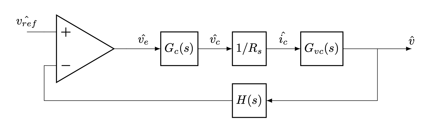
Starting on the right, the output voltage is passed through the sensor block H. This is just a resistor divider with a gain of 1/170 for this converter. This is subtracted from the LM5155 voltage reference, creating an error signal. The error signal is fed through the compensation network, and then voltage is converted to a current value by the resistance of the sense resistor. The resulting current control signal is fed into the current programmed controller and the current-to-output gain Gvc determines the feedback output voltage. Determining the structure of Gvc (all its poles and zeros) is the hard work of the analytical path.
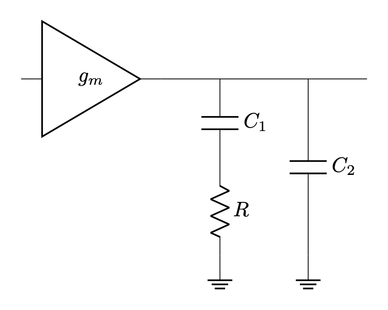
Current mode controllers generally need a simple compensation network, called a type II compensator, that is just a shunt resistor and capacitor in series. This has an origin pole and a zero at the RC corner frequency. An optional high frequency pole is added by putting another capacitor in parallel with the series branch.
To determine Gvc, the first step is derive a small-signal AC model of the converter. This can be obtained through my preferred method of state-space averaging, or by circuit analysis using an averaged switch model.
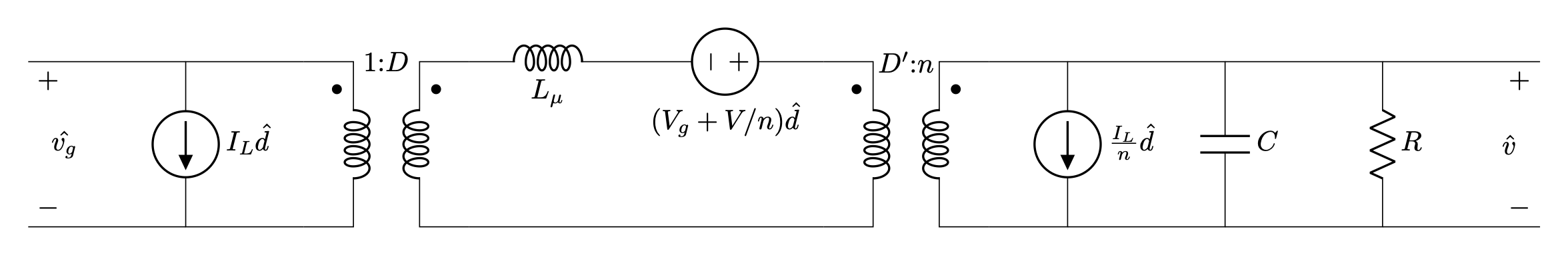
From the small signal model, the control-to-output-voltage and control-to-inductor-current transfer functions can be solved from the state-space analysis results or read off the AC small-signal circuit. These are voltage mode transfer functions though, and what's needed is the current mode control-to-output-voltage transfer function. Converting them requires parameters of the current mode modulator (why I said that a large artificial ramp affects the stability of the system). Sounds like a lot of work? It is.
For the flyback converter, the current-mode control to output transfer function can be written in the form:
This means there a DC gain Gc0, a single real zero in the right hand plane, and a pair of resonant poles. In the following, L is the transformer magnetizing inductance, C is the output capacitance, and R is load resistance. These are:
The modulator parameters are:
Choosing the compensation network
With that out of the way, how to actually get those magic R and C values? For stability, it's important to design around the right hand plane zero in the transfer function. A way to understand a right hand plane zero is to imagine a car that, when you tap the brakes, very briefly speeds up before slowing down. If that blip of speed happens and is over before you can notice and react, all is fine. But if you do have time to notice, you panic, hit the brakes harder, which makes the car speed up again ...
To prevent this situation in this power converter, the control loop bandwidth needs to be significantly lower than the RHP zero frequency, so the loop will not try to correct for it. Using the parameters for the converter that will yield the lowest frequency (5 V input, pushed to 40 mA output just for headroom), the RHP zero frequency is 45 kHz. To meet this criterion, the crossover frequency (where the gain of the feedback loop is 0 dB) is usually kept below 1/5 the RHP zero frequency. In this case, I rounded it to 8 kHz as the target crossover frequency.
Another requirement for stability is the phase margin criterion. This says that a system is stable if, at the crossover frequency, the system's phase is greater than -180°. The difference between the system's phase at crossover and -180° is the phase margin, and typically a figure of around 60° is a good target.
The choice of the compensation resistor will adjust the gain at crossover, and the zero from the RC corner frequency will give some control over the phase. One can figure out the ratio of the uncompensated gain at crossover, determine the gain adjustment required to hit 0 dB, scaled by the LM5155's amplifier transconductance ... meh, just give the job to a computer, it will happily descend gradients for you and nail both the crossover frequency and phase margin. I wrote a python script that uses scipy's optimize framework to iteratively select the exact values. I also added the optional high-frequency pole in this script - the choice of frequency is arbitrary, but placing the HF pole at the RHP zero frequency is one choice.
Here's the output of the script:
Type II OTA compensator
Compensation network for crossover at 8000 Hz with 60° phase margin: R_c = 1504.96 Ω, C_c1 = 6.87088e-08 F, C_c2 = 1.80016e-09 F
Chosen compensation network: R_c = 1.5e+03 Ω, C_c1 = 6.8e-08 F, C_c2 = 1.8e-09 F
Crossover at 8e+03 Hz, phase margin: 60°
So that's the network I'll use: R = 1.5 kΩ, C1 = 68 nF, and C2 = 1.8 nF. The script also plots the Bode chart of the compensated feedback loop. Edit: I later found my script left out the PWM gain factor. The correct numbers for this configuration are R = 11 kΩ, C1 = 10 nF, and C2 = 270 pF.
Experimental validation of the loop gain
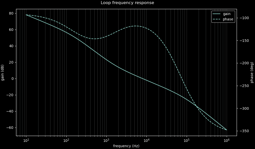
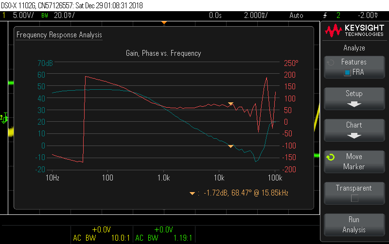
Sophisticated mathematical models are one thing, but useless if you can't validate them. One method to analyze the feedback loop in circuit is by injecting a voltage signal into the feedback line using a function generator and observing how that signal is coupled to the output. My oscilloscope (Keysight 1102-G) has a frequency response analysis tool that produces a Bode chart similar to above by comparing the voltages at both channels as the function generator sweeps through a frequency range. If it works right, the plot will look something like this, taken from an older project.
To do this, the signal has to be injected without disturbing the DC value of the feedback line. Here is the sketch of a voltage injection circuit that doesn't break the feedback loop.
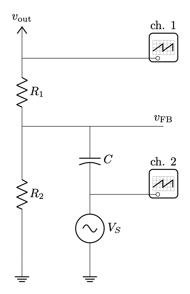
At DC, the feedback voltage is just the output voltage scaled by the resistor divider. The capacitor C is large, say 1000 µF, and can be thought of as a short at any frequency above DC. The source generator VS is a typical function generator with 50 Ω impedance. The total impedance of this branch should be small in comparison to R2 (10 kΩ in the design), which means the DC level of FB is unchanged, but the AC component is almost entirely driven by the function generator. Probes connected to the output voltage and the output of the function generator should be tied to the same ground point, and then the frequency response analysis tool can be started. Because of the high gain of the error amplifier in the LM5155, the voltage level required from VS is very small, and can be more precisely set by coupling VS across a 1/1000 resistor divider.
In the board design, a pair of headers allows the attachment of a function generator, labeled J5 and J6 on the board.
Discussions
Become a Hackaday.io Member
Create an account to leave a comment. Already have an account? Log In.