 James Wilson
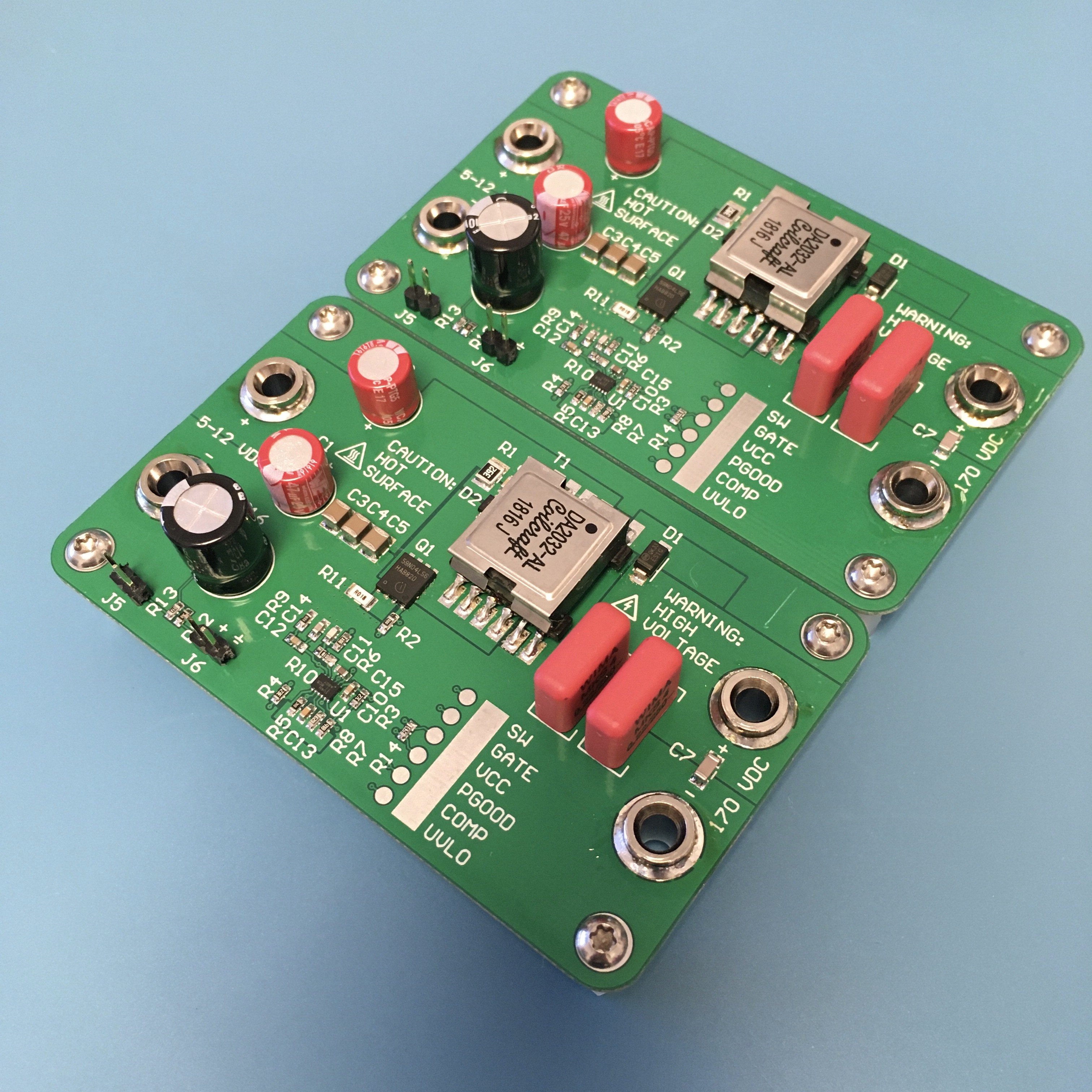
The boards were produced by JLCPCB and in my hands within a week, very nice considering concerns about the global economy at the moment. I assembled identical boards, one as a reference and the other to be poked and probed, and sacrificed if needed.
Load board
I don't have an electronic load, which makes testing power supplies a lot easier. Even if I did, most general purpose e-loads aren't set up well for the corner case of high-voltage, low-current power. Even though this board sources less than 10 W, I'd need an overspecced e-load just to handle the voltage rating, or use something like an SMU (even more expensive).
So along with this board, I also had a second board made that lets me adjust the load manually in steps. Each switch on this board adds a branch with two 1 W 68 kΩ resistors in parallel, or 34 kΩ. 170 V into 34 kΩ gives 5 mA per switch, so the output current can be stepped from 0 - 50 mA.

Startup transient
Does it work? Connecting the inputs to a bench supply the and output to a multimeter, I anxiously flipped the switch, and heard ... the satisfying click of my multimeter's autoranging relay followed by a reading of 169 V! Connecting the load board, I flipped the switches and watched the voltage remain rock-steady as I pushed the load current to 50 mA. Satisfied that nothing was going to give off smoke, I started characterizing the board on an oscilloscope.
Setting a long time base, I examined the startup ramp transient. At 5 V and 12 V input voltage, it looked identical.
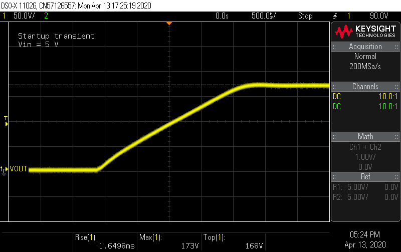

The startup time seems fixed. Well, there was that soft-start feature... The soft-start ramps up the feedback control voltage as the soft-start capacitor charges to 1 V. How does the SS pin voltage and ramp time compare to the output voltage? I set the rise time measurement on the output voltage to measure 0 to 100% (usually rise time is cited as 10 - 90%) and an absolute rise time for the other channel with a limit of 1 V.
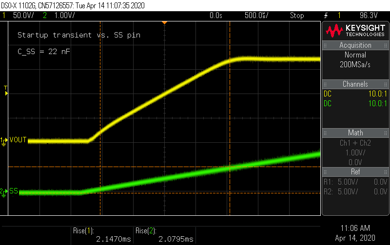
10 µA into 22 nF rises to 1 V in 2.2 ms, so that looks right. What happens if I replace C_SS with something larger, like an extra 68 nF from the compensator circuit? I'd expect the rise time to go to 6.8 ms...

Bingo! I kind of like this a bit more. The slower rise time appears to eliminate the mild voltage overshoot that's noticeable with the original 22 nF choice.
Load transient
Next, how well does the controller handle a sudden change in load? In the simulation, I used a 15 mA load step, but try as I could, there's no way to flip 3 switches at exactly the same instant, so I only captured the step load transient for a 5 mA step. These are AC-coupled captures, so going to zero means a return to regulation.
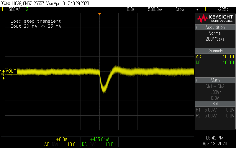
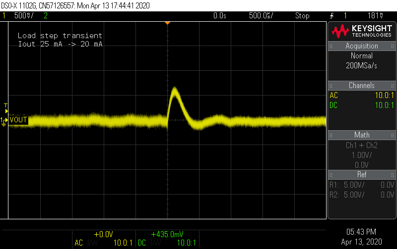
In the design phase, I used a crude estimate of the converter's output impedance to size the output capacitance to limit the load transient to 1 V at a 15 mA load step. In simulation, the result looked closer to 2 - 3 V. Here the transient is about 700 mV for a third the size of the load step, so that the simulation looks like it's predicting things well.
Another way to understand the load transient is look at the feedback loop response. I added a circuit to permit injecting a function generator signal into the feedback loop. Unfortunately, it didn't work as planned. Once the jumper to ground is closed, the large capacitor (1000 µF) pulls down the FB line voltage causing the output voltage to spike. This stresses all the components and destroyed one of the test boards very quickly. The board can't withstand the high voltage during the charging time, even if the coupling capacitor is reduced to 100 µF. It's disappointing this part doesn't work after all the theoretical work that went into designing the compensation network. There are other ways to make measurements of the loop gain, but they involve breaking the feedback loop and will require a board respin. Wary of destroying my remaining board by a careless short of one of those headers, I removed those components for my remaining tests.
Output ripple
Output ripple measurements were made by probing directly across C7 in AC coupling mode. There's definitely some high frequency component that's modulated with the lower frequency ramp up and down.
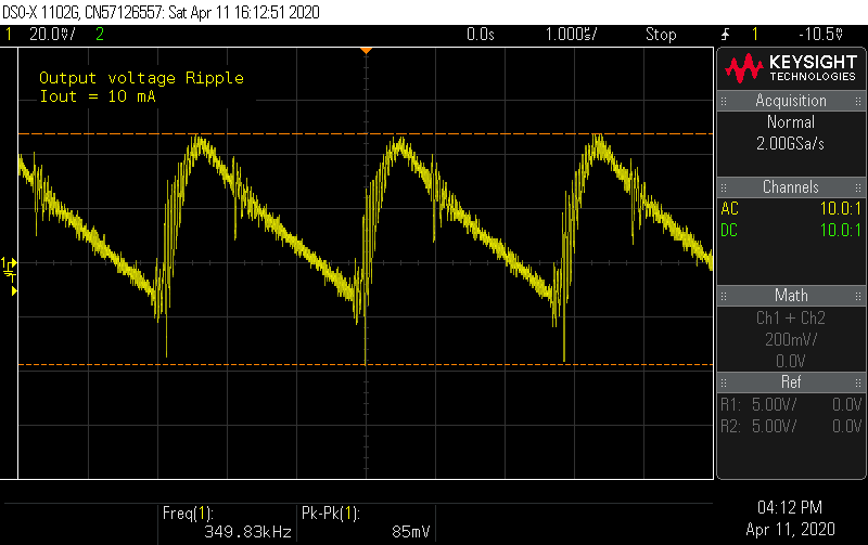
At 30 mA load, these spikes get larger, but overall the ripple is manageable at less than 300 mA. From the output ripple formula, at 30 mA, the output ripple should be about 150 mV, which if you ignore the ringing not predicted by the formula, looks about right on.
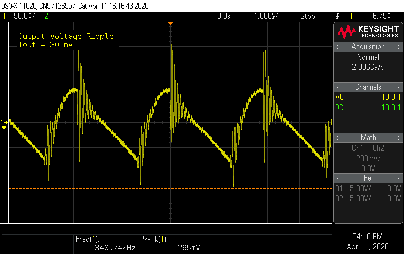
Is the 10 nF capacitor C7 doing anything? Should it get to keep its job? Let's remove it and see what happens.
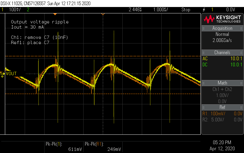
Seems the 10 nF ceramic capacitor really does help after all.
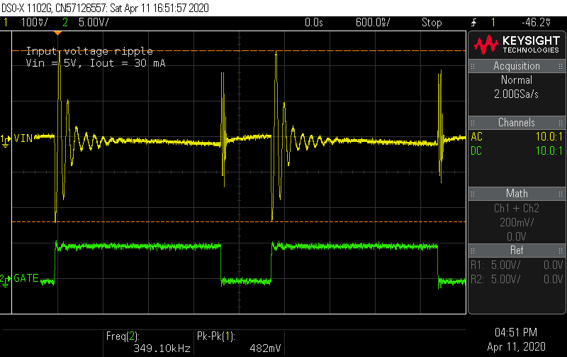
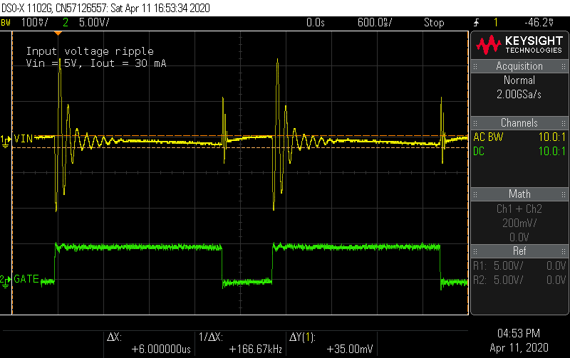
Input ripple
Probing directly across the input terminals, I measured the input ripple. There are ringing waveforms at the edges of the switching cycle, but the low frequency ramp appears to have a peak-to-peak amplitude of about 35 mV, which was close to the design target.
What effect do the three ceramic caps C3, C4, and C5 have? Removing the last one shows some mild effect.
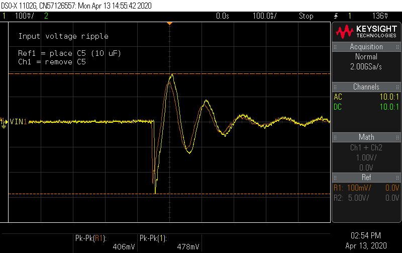
I squeezed two 1206 10 µF caps into the space of one 1210 and measured the result. It appears the point of diminishing returns has been reached.
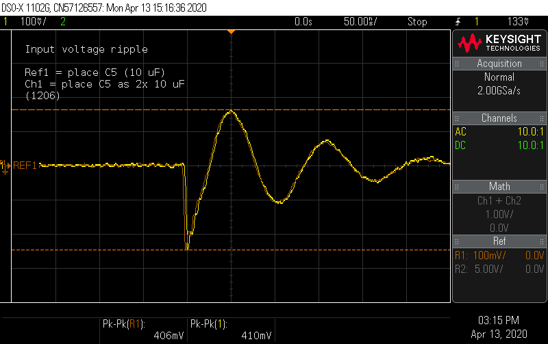
What about additional capacitance in a lower decade? I tried the same trick with some 1 µF 0805 caps.
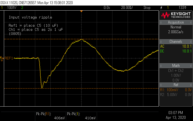
Unfortunately, it appears additional capacitance cannot reduce the spikes at the input. The more I looked at things, the more I suspect that a poor layout choice might be responsible. When the switch turns on, the source current instantly jumps to the average inductor current. Small capacitors will be the lowest impedance path for a sharp current step, so the current will prefer to go through the bank of ceramic capacitors. Under load, the inductor current is substantial and any stray inductance in this loop will cause sharp voltage spikes. Inductance is related to loop size, and the placement of the capacitors forces a sizeable loop on the top layer. Current can also flow on the bottom layer under the path from T1-Q1-R11, around the trace that cuts the ground plane, and then double back to reach C3-C5. It's hard to guess what is the actual lower inductance path.
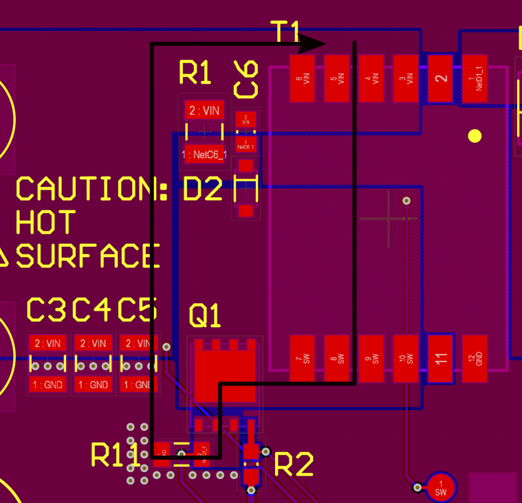
A better layout would be to move C3, C4, and C5 directly adjacent to the transformer pads and let the current flow underneath the path on the bottom layer, which greatly reduces the loop size. This too will require a board respin.

Discussions
Become a Hackaday.io Member
Create an account to leave a comment. Already have an account? Log In.