 James Wilson
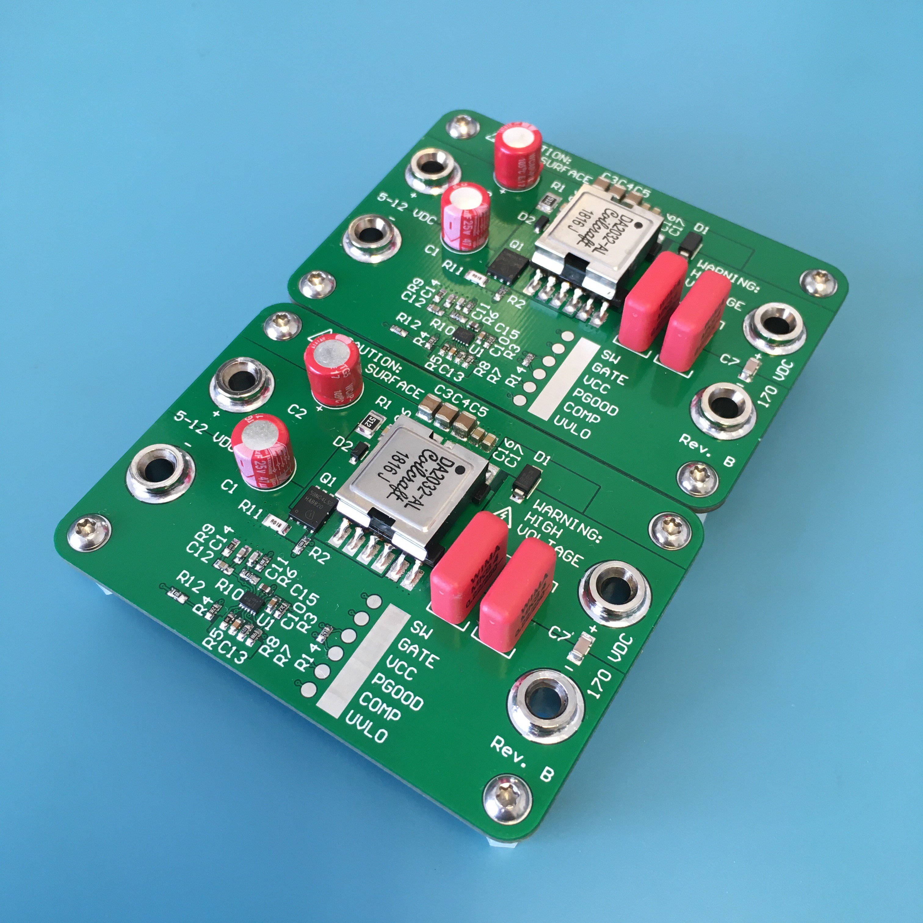
The rev. B boards arrived and I assembled three of them with the remaining parts. The differences are subtle:
- the input capacitors have been moved adjacent to the transformer, with a clear return path on the bottom side ground pour
- loop gain circuit was scrapped and replaced with a single 20 Ω series resistor for use with an injection transformer
The resulting board is slightly smaller.
Experimental validation of the feedback loop bandwidth
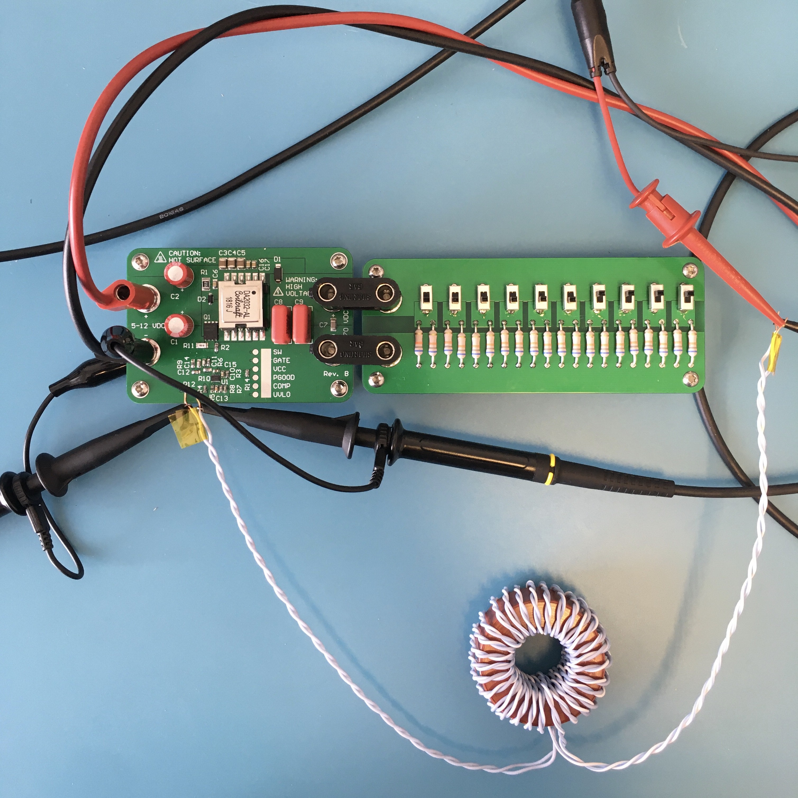
After all the modelling done in a previous section, how good was it? Following the procedure in AN-1889, I connected a 1:1 injection transformer across R12. This transformer is a homebrew device with a bandwidth of 40 Hz - 2 MHz. One side was connected to my scope's built-in function generator, and the other side was soldered across R12. I used the oscilloscope's frequency response analysis tool to produce a Bode chart of the converter's feedback loop.
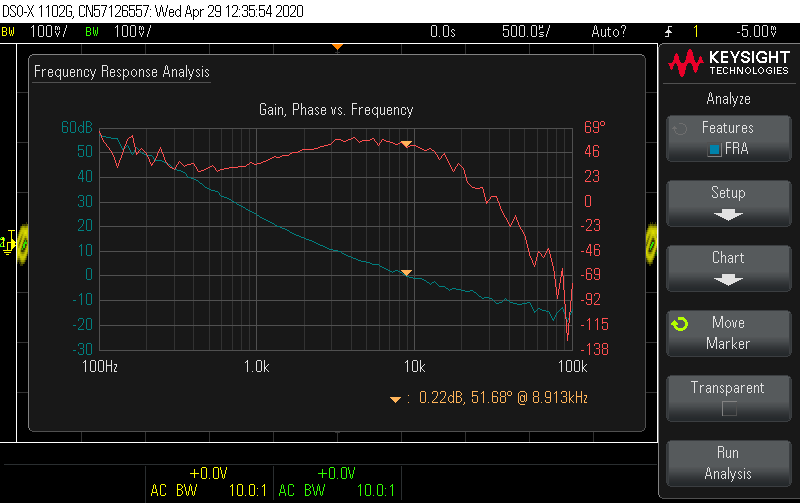
For the original configuration in the design work (fs = 350 kHz, Vin = 5 V, Iout = 30 mA), the measurement shows crossover is at about 9 kHz with a 51° phase margin. The model prediction was crossover at 8 kHz with a 60° phase margin. The shape of the gain and phase curves shows good agreement to the model. If I were going to keep using this configuration, I might tune the compensator's zero frequency to get a little closer to the target phase margin.
For comparison, here is the model prediction:

One of the changes I explored was dropping the switching frequency to improve efficiency. The LM5155 can go as low as 100 kHz, and I made an experiment with fs = 150 kHz earlier, noting that the compensation network might need adjustment. Now that I have the means to measure the loop from a point of relative stability, why not try the practical approach of tuning the components from a real circuit? After the amount of work that went into modelling the CCM transfer function, I'm in no hurry to do a model for DCM if only a minor adjustment is required. The remaining boards run at 100 kHz, so I repeated this experiment at Vin = 5 V, Iout = 30. The results are almost identical.

To see how DCM affects the loop dynamics, next I put the converter as deep into DCM as I could by running it at the highest input voltage and lowest current (12 V input and 5 mA output). Here the crossover frequency drops to shy of 5 kHz, with a healthy phase margin.
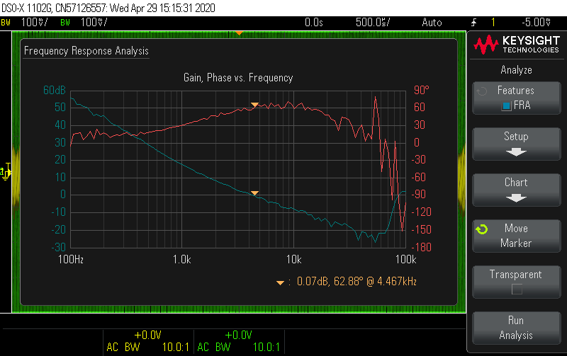
Before wrapping up this test setup, I also looked at middle-of-the-road configuration: 9 V input, 25 mA output current.

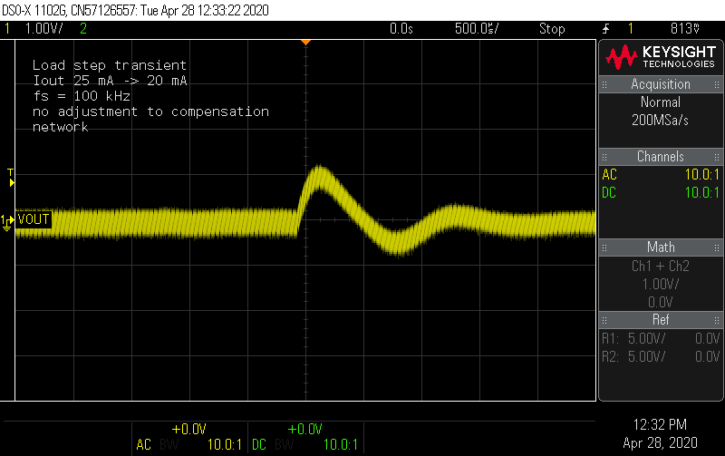
My conclusion is to stick with the current compensation network. Often what happens with DCM is the right-hand plane zero gets kicked out beyond the switching frequency, so using 1/10*fs is a common choice for the crossover, and this shows it's already set close to 10 kHz with a good phase margin. The step load transients (measured on rev A adjusted to 100 kHz) show good response in the time domain as well.

Revisiting voltage ripple and primary snubber
One of the changes was to improve the layout around the input capacitors. For comparison with rev. A, this time I measured the input ripple across the input capacitors, both converters operating at 100 kHz. This shows about half the ripple, with the smaller 1 µF capacitors taming some of the spikes.

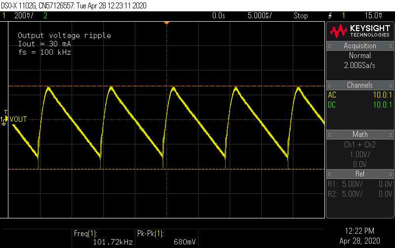
A lower frequency means increased output ripple since I didn't change the output capacitance. At 100 kHz, the voltage ripple increases to 1.4 V (p-p) at full load. This is still less than 1% of the DC level, and Nixie tubes do not need flat DC. Nonetheless, this could still be improved by increasing capacitance, with some possible adjustment required to the feedback loop. In this this package, film capacitors up to 470 nF are available, which would roughly double the output capacitance. For the target application, I'm fine keeping the pair of 220 nF caps.
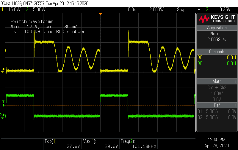
While looking at rev. A modified to run at 100 kHz (with the snubber removed), the switch node voltage saw peaks approaching 40 V, presenting concerns given the Vds rating of the MOSFET.
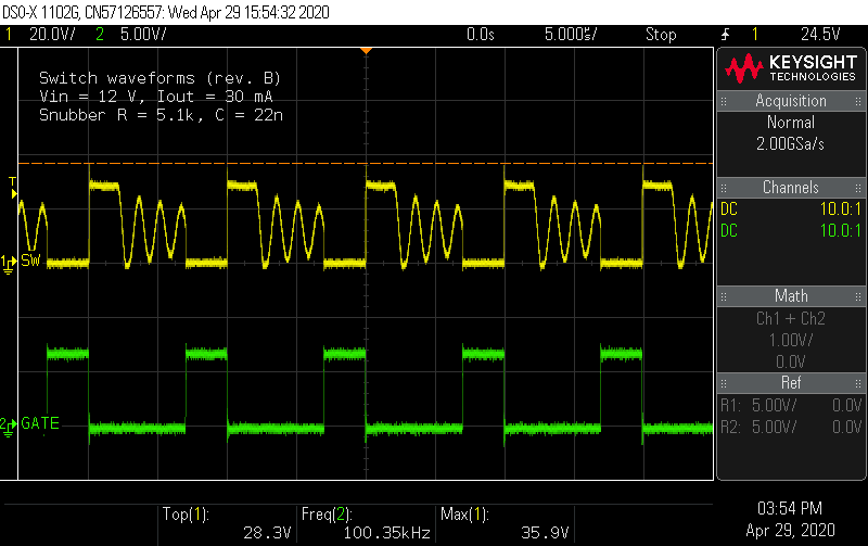
I placed the snubber components for the rev. B boards, and measured the switch node voltage at the highest level configuration (12 V input, 30 mA output). This keeps the switch node voltage at 90% of its rating.
Final efficiency measurements and conclusion
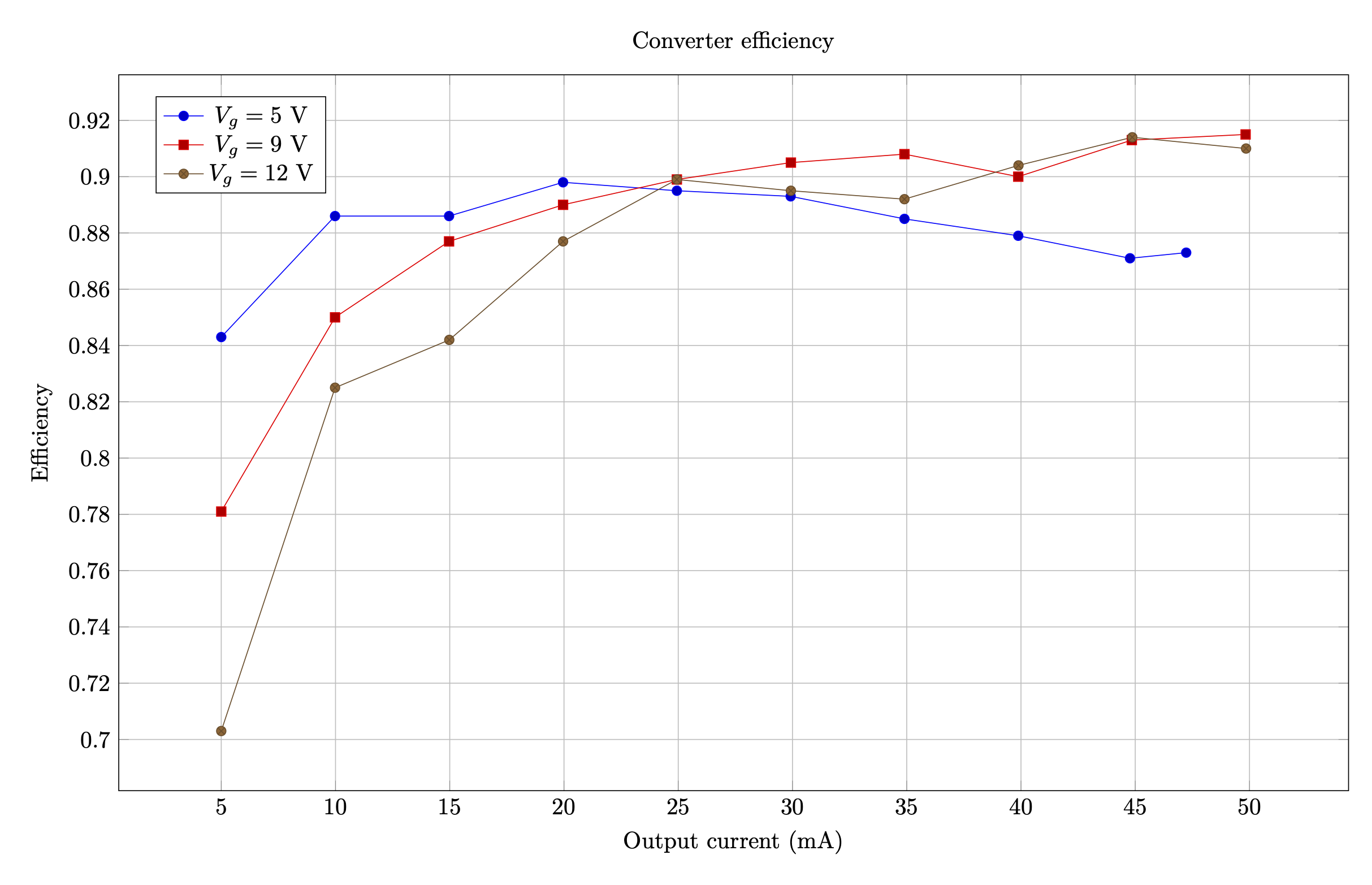
The efficiency measurements at 100 kHz switching frequency show a slight improvement over the previous experiment at 150 kHz. The converter is capable of nearly 90% efficiency over a wide range of conditions, peaking at over 91%. The end of the curve at 5 V shows that current limiting kicks in at Iout = 45 mA, as a precaution against saturating the transformer.
With that, and the end of April arriving, I think it's time to call it a wrap on this project. All of the characteristics of this flyback converter have been verified on the bench. Lastly, just to show it does in fact light Nixie tubes:

Discussions
Become a Hackaday.io Member
Create an account to leave a comment. Already have an account? Log In.