Whenever I design a board, I optimize as much as possible. Layer count, part count and even part location can play a big role in how much assemblies cost later down the road. In this article, I go into depth about the decisions I made when designing the nRF9160 Feather. Let’s do this thing!
The Essentials
The first part of the process was determining what stays and what goes. In my case, as this is a traditional Feather, the design needed some functionality. Things like:
- A built in Li-Poly charger
- USB for charging and USB-to-UART transfer
- Programming connections for SWD/JTAG
- External flash storage. (The nRF9160 has 1MB of flash but more external non-partitioned space is always good!)
- A way to get the device into super low power.
- And, of course, the capability to support the nRF91 + antenna connections.
This by no means is a short list! Each feature has its own nuance which is important when trying to mash them all onto a 22.86x50.8mm board.
CAD of Choice
After using many CAD packages (and owning some) I go back to Eagle every time. I also use it to track my library and my parts. Every time I add a part, I enter the part data like MPN, Description and more. That makes exports into a shopping cart or even into a MRP/PLM tooleasy peasy.
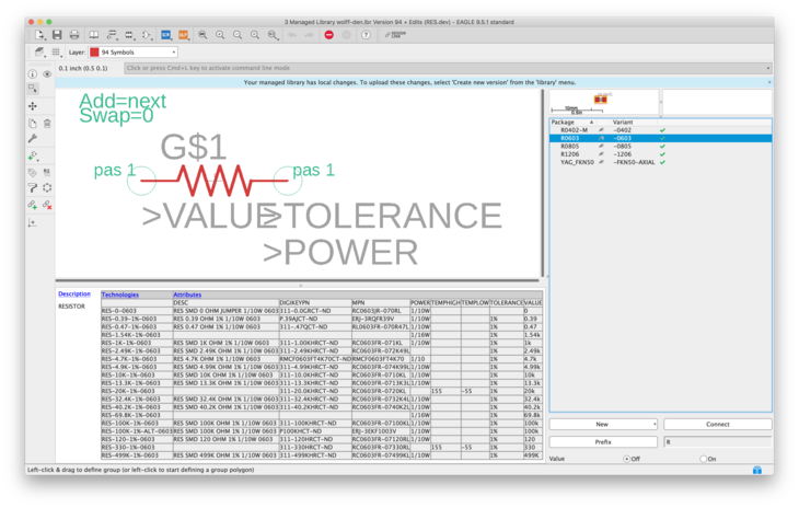
I’ve described my methodology in the past. You can check it out here.
Stack It Up
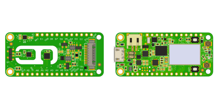
Placing parts is the first step. It’s a helpful guide to what will fit where. I actually started with a 2 layer board and then upgraded to a 4 layer later on due to the increased density.
In comparison with the Air Quality Wing, there’s little room on the top layer! It’s one of the more complex boards i’ve designed from concept to fab. In the past i’ve used layout services but doing it myself was going to be cheaper and faster!
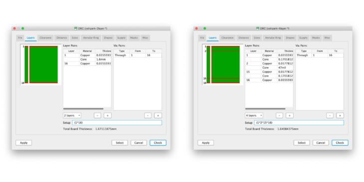
Thanks to OSH Park’s fab design constraints, I didn’t have to think much about the stack up. The important thing is that you’ll want to use what ever your board house deems “standard”. Don’t thinking about it too much though, or you may get lost in the list of what they can do. (OSH Park has a similar list but it’s much more concise. We’re not building rockets here.. or are we?)
Here’s what a standard stack up looks like for both OSH Parks 4 and 2 layer .ulp files. You can get them here if you’re interested in a good starting point for your own designs!
Placement and Constraints
When placing a new board, you always want to place parts as recommended by the various ICs you chose. i.e. placing a bypass cap as far away from the chip you’re using will not do much at all!
For example, TI recommends you keep the bypass caps and inductor as close to the DC/DC as possible. Here’s a screenshot of their layout recommendations in the datasheet:
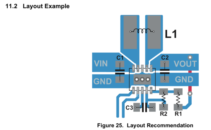
Source: TPS63031 datasheet
You can see that the input and output copper is fairly chunky. I’ve also drilled a ton of vias which decreases the resistance in layer transitions.
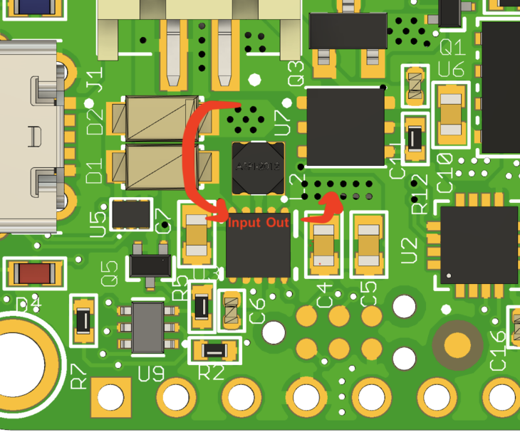
I’m a polygon maniac so I use it for all shapes that I can’t fix with a simple trace. Additionally, I will almost always turn off thermals for these shapes. Otherwise you lose most of the copper involved. There are some cases where you will have to tweak this setting though! This is true especially if you attempt soldering a pin thats tied to a large chunk of copper (i.e. a hefty ground plane). In that case, if you don’t use thermals, you may end up with cold solder joints!
You can also see that i’ve kept most of the power related parts clustered in the same area.
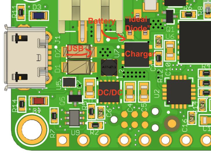
This decreases any parasitic resistance between all the important power related parts. Despite being very close, many of the power traces transition to an inside layer. Let’s take a look.
Setting Up the Layers
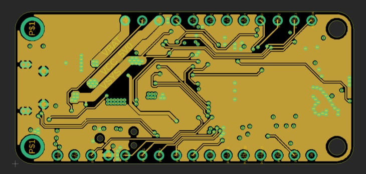
In Layer 2 I’ve routed some of the power signals from the top side through this layer. You can see there’s battery, 5V to the 5V pin and VSYS which is the combined input to the DC/DC. I almost always route these chunky power traces before I do the smaller stuff. They’re much more important and should have as a direct route as possible. (this goes back to keeping trace resistance low which is 👍 for power delivery)
You can also see that i’ve done routing of many other miscellaneous signals on this layer. I used the convention of connecting the outside through holes to this layer. This allowed for a more direct connection to pins on the nRF91.
Finally, if you look closely there’s a set of traces coupled together. These happen to be the USB D+/D- signals.
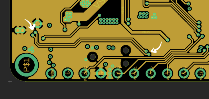
This board is not doing anything crazy high speed so routing from the top to the next layer down was ok in my book. In general though, especially for differential signals, avoid the layer transitions!
Similarly for the top and bottom layer, i’ve used a copper fill connected to ground. That way it’s easier to make a ground connection. This also helps considering Layer 2 is all chopped up by the traces, vias and chunky power traces!
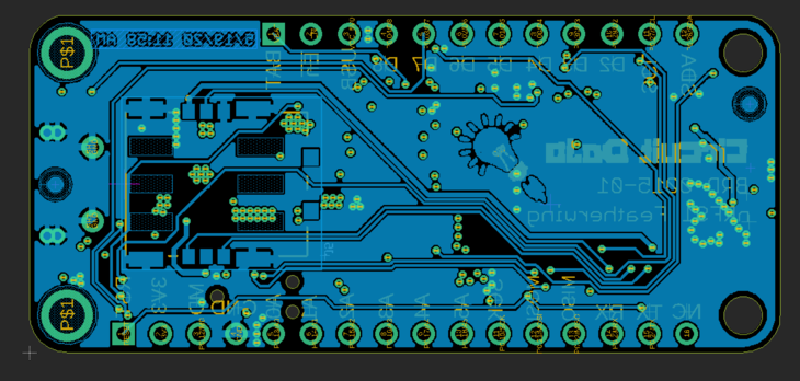
On the bottom layer there is only one surface mount component. If I had the ability to, I would have put it on the top side. Unfortunately the SIM holder is way too bulky!
If it was a possibility that would have saved about $100+ in stencil cost. As you can imagine you can save some costs on SMT assembly as well! For this side, i’ll skip Automated Optical testing since there’s only one component. Hard to get that one wrong!

As for the other inner layer, it’s simple a layer for 3.3V only. If a part needs 3.3V, drill to the layer below for power. There’s no futzing with power traces. It’s clean and makes signal routing efficient!
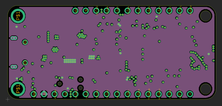
The only thing to watch out for is all the non-connected vias turning the layer into swiss cheese. Imagine if I had 2x the vias in the above capture. That would cause the layer to not be as thick and contiguous. This could lead wreak havoc on your circuits. Fortunately this design is simple enough where that is not a huge concern!
Don’t short power to ground.
As I had mentioned in my previous post, I ran into some issues where I did not define my slots correctly. Fortunately, the only part that was using slots was the USB connector. If you zoom in on the 3V3 layer you can see now it’s fully isolated. That way this problem won’t happen again!

To construct a slot, use the Milling layer (Layer 46 in Eagle) plus some through hole “pins”. OSH Park merges these all together so there no need to worry about overlapping drill passes.
Shutting Things Down
One of the more important things about the design is the ability for the board to turn off. That’s right, completely off.
My thinking went to two options of handling this power down state:
- Turn the power supply completely off. Only power supplied to an “always on” part acting as a supervisor.
- Or, turn off the switching power supply and run most of the circuitry off of a parallel LDO. The circuitry would then be run in a low power/standby state.
The thought experiment lasted a while. Even up until I was about to send Proto2 to fabrication! I decided to go with option 1 over option two because it will draw the least amount of power when off. Plus it’s the most simple! The second option required a significant amount of tweaking and hacking.
On a comparison level I was looking at something like 1-2µA in option 1 versus about 8-10µA in option 2. I’ve yet to measure and test but these principles have been time tested by others that have come before me.
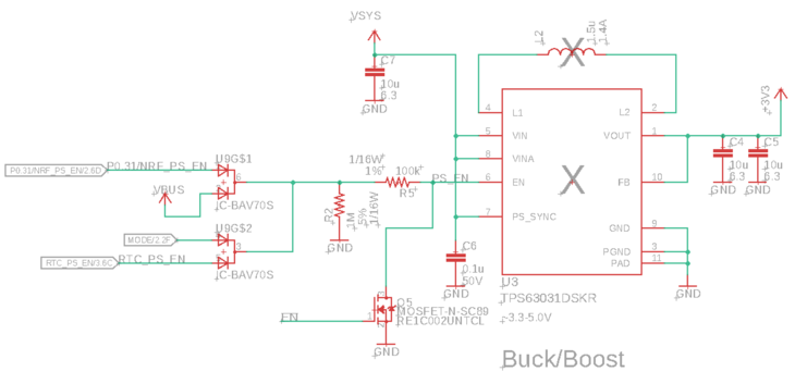
Here’s what the DC/DC circuitry looks like. As you can see there are multiple parallel diodes providing a signal to the EN pin. All these individual sources can keep the nRF9160 Feather powered.
One of those sources is an RTC (Real Time Clock). This chip draws less than 1µA and uses a 32kHz crystal to generate accurate time. It has some timer and alarm features which are perfect for waking up the DC/DC at a programmed timeframe.
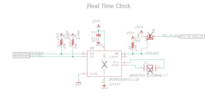
Additionally, we can use the GPIO on the nRF91 to keep the power supply on. Once it’s ready to sleep/shutdown it releases that pin.
For field deployments, the low power state is more important than the powered state. That’s because you spend most of your time in this state. A difference of a few µA can lead to a difference of years in operation. And that’s the problem i’ve tackled here in the nRF9160 design.
RF Circuitry
The RF circuitry for this board was not straight forward. There are still some open questions about how it would perform. Since I’m located in the USA, I will only be able to test an LTE based solution. (Though the nRF9160-SICA is able to do both!)
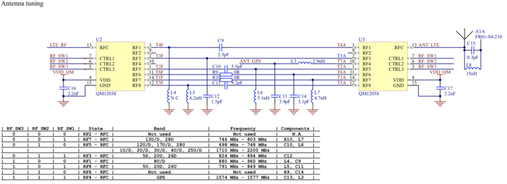
From Nordic’s Thingy91 Schematic
If you want to see something cool, take a look at Nordic’s Thingy91 reference design. You can see that they multiplexed the matching circuitry for each band. There are pins on the nRF9160 which are 100% dedicated for driving these multiplexers. Unfortunately, as you can see below, there’s little room for that!
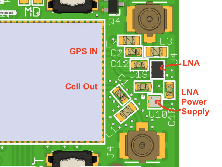
The most important thing here was to include GPS along with celluar. Why have a nRF9160 board, which has GPS, but no way to use it? Silly no?
The GPS signal uses a separate LNA + Power Supply for amplification stage. This seems to be common practice across Nordic’s reference designs. Here’s what mine ended up looking like:
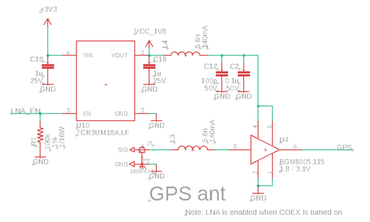
The cool thing was discovering that I could use COEX0 pin to drive the power and enable for the LNA. I’ll test Proto2 in the coming weeks. I’ll be sure to share my findings with you.
Open Source
Anyway that’s the current state of the nRF9160 Feather! Proto2 is well on its way. With that some more debugging and testing!
I know you must be wondering, can I get my hands on this source? The answer is: soon! I’m excited to say that the design will be fully open source when it launches with Hackster and GroupGets. As you can tell, there’s more to do but i’m excited to get it in your hands soon! If you’d like to be one of the first to know about availability, sign up for the mailing list here.
Next Post
Next weeks post will be detailing setup of Nordic’s nRF Connect SDK. So stay tuned for that!
 Jared
Jared
Discussions
Become a Hackaday.io Member
Create an account to leave a comment. Already have an account? Log In.