 Abduulah Omran
Just finished the first version of the Schematics and PCB design .
yet i think the PCB need some review do to many reason , firstly because i lack experience in PCB Deign , secondly is that this is RF PCB, so there is some guidelines to follow.
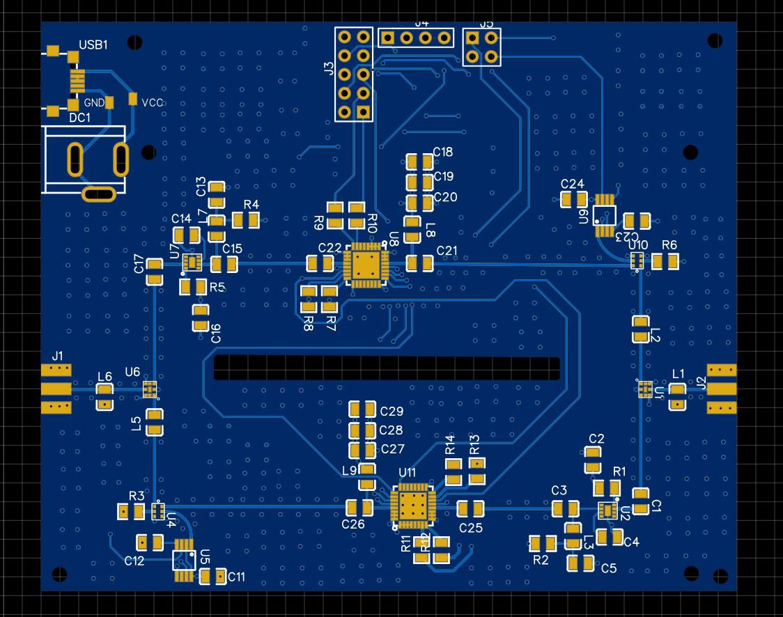
This PCB is design foe OSHPARK 4 layer pcb .
I followed the common rules of RF PCB designs .
1- Use 50 Ohm Traces ( OSHPARK 4 Layer Stack ) .
2-Curve the RF traces or use slanted corners .
3-4 layer PCB .
some others i didnt follow :
1- I used 0805 SMD components , because it is easier to solder.
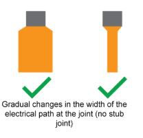
2- did not pay attention to the stub pads of smd components on the RF trace. it spouse to increase gradually until it reach the right size
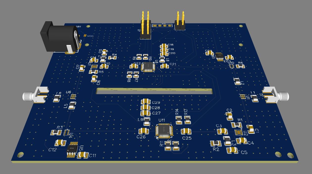
Finally this is a 3D view of the PCB . and i will attach a Schematic and update the Block Diagram.
I can refer any one who is interested in RF PCB to watch Micheal Ossmann YouTube video about RF circuit Design.
Discussions
Become a Hackaday.io Member
Create an account to leave a comment. Already have an account? Log In.