 mbsg99
Committed to providing one-stop electronic hardware services for over a decade, Seeed Fusion has the expertise and engineering insight to deliver streamlined PCB assembly at low costs and is equipped with a wide range of value-added services and capabilities. Check out their website to know about their manufacturing capabilities and service.
To available Seeed Studio Sevices: https://www.seeedstudio.com/prototype-pcb-assembly.html
About Hardware:
1.CA3130 Op-Amp
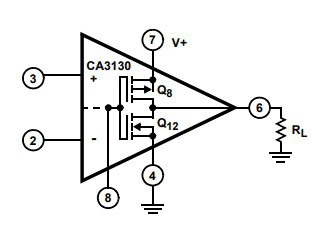
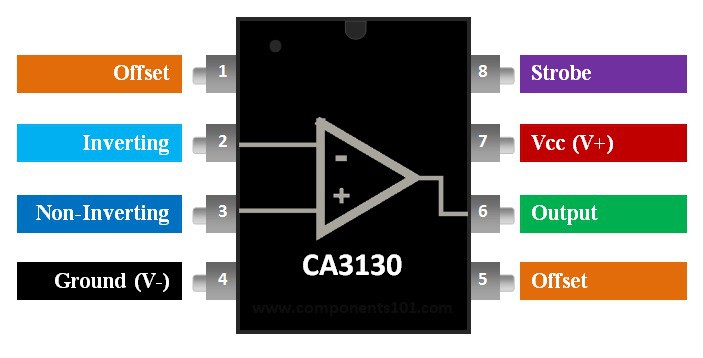
The CA3130 can work in a Single supply voltage or in a dual supply mode. For now let’s concentrate on the +5V supply voltage circuit since this is the most used design for digital circuits. In this type, the VCC+ (pin 8) is connected to +5V supply voltage and the VCC (pin 4) is grounded to hold it at 0V potential.
CA3130 Specifications
- Op-amp coupled with MOSFET at output
Wide power supply Range
- Singe supply – 5V to 16V
- Dual supply – ±2.5V to ±8V
- Input Terminal current: 1mA
- Maximum Output Voltage: 13.3V
- Maximum source current: 22mA
- Maximum sink current: 20mA
- Supply current: 10mA
- Common Mode Rejection Ration (CMRR): 80dB
Applications
- Frequency Generator/Distorter
- Mobile jammers
- Voltage follower circuits
- DAC circuits
- Peak Signal/Noise detectors
- Oscillator circuits
2. BC547
_TZvDdp36br.jpeg?auto=compress%2Cformat&w=740&h=555&fit=max)
BC547 is a NPN transistor hence the collector and emitter will be left open (Reverse biased) when the base pin is held at ground and will be closed (Forward biased) when a signal is provided to base pin. BC547 has a gain value of 110 to 800, this value determines the amplification capacity of the transistor. The maximum amount of current that could flow through the Collector pin is 100mA, hence we cannot connect loads that consume more than 100mA using this transistor. To bias a transistor we have to supply current to base pin, this current (IB) should be limited to 5mA.
When this transistor is fully biased then it can allow a maximum of 100mA to flow across the collector and emitter. This stage is called Saturation Region and the typical voltage allowed across the Collector-Emitter (VCE) or Base-Emitter (VBE) could be 200 and 900 mV respectively. When base current is removed the transistor becomes fully off, this stage is called as the Cut-off Region and the Base Emitter voltage could be around 660 mV. BC547 as Switch
When a transistor is used as a switch it is operated in the Saturation and Cut-Off Region as explained above. As discussed a transistor will act as an Open switch during Forward Bias and as a Closed switch during Reverse Bias, this biasing can be achieved by supplying the required amount of current to the base pin. As mentioned the biasing current should maximum of 5mA. Anything more than 5mA will kill the Transistor; hence a resistor is always added in series with base pin. The value of this resistor (RB) can be calculated using below formulae. RB = VBE / IB Where, the value of VBE should be 5V for BC547 and the Base current (IB depends on the Collector current (IC). The value of IB should not exceed mA. BC547 as Amplifier A Transistors acts as an Amplifier when operating in Active Region. It can amplify power, voltage and current at different configurations. Some of the configurations used in amplifier circuits are
Common emitter amplifierCommon collector amplifierCommon base amplifierOf the above types common emitter type is the popular and mostly used configuration. When uses as an Amplifier the DC current gain of the Transistor can be calculated by using the below formulae DC Current Gain = Collector Current (IC) / Base Current (IB).
3. BC557
_DGAnhWgKak.jpeg?auto=compress%2Cformat&w=740&h=555&fit=max)
Features / Technical Specifications:
- Package Type: TO-92
- Transistor Type: PNP
- Max Collector Current(IC): -100mA
- Max Collector-Emitter Voltage (VCE): -45V
- Max Collector-Base Voltage (VCB): -50V
- Max Emitter-Base Voltage (VBE): -5V
- Max Collector Dissipation (Pc): 500 Milliwatt
- Max Transition Frequency (fT): 100 MHz
- Minimum & Maximum DC Current Gain (hFE): 125 to 800
- Max Storage & Operating temperature Should...
 ensgoldmine
 Sagar 001
 Lithium ION
 kamalkedin123