 Electroniclovers123
Application
Designed for low voltage, high speed power switching applications such as Switching Regulators converters, uninterruptible power supply, dc/dc converters for telecom, industrial, and lighting equipment, solenoid and Relay Drivers. It is generally fancied every commercial-industrial purposes at power dissipation levels to roughly about 50 Watts.
IRF640 power MOSFETs are particularly made for purposes like relay drivers, switching convertors, switching regulators, motor drivers and high power bipolar switching transistors drivers that need high speed and low gate drive power.
Specifications and features of IRF640Description
IRF640 is a power MOSFET of the N- channel enhancement mode silicon gate power field effect transistor. It is made using the strip layout-based mesh overlay process. This is a technology that complements and enhances the performances than other standard devices. It simplifies assembly and reduces the risk of accidental short circuit in crowded monitor Printed Circuit Boards’.
The reason why it’s is widely embraced in many applications is that it has low thermal resistance and low package cost.
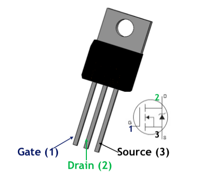
IRF640 Power MOSFET has got three terminals:
G: Gate
D: Drain
S: Source
Once the drain is linked to the positive power supply and the source is connected to the negative power supply, the voltage between the gate and the source is zero and the channel is nonconductive hence the tube is cut off. Once a forward voltage VGS is exerted between the gate and the source, and the VGS is greater than or equal to the opening voltage VT of the tube; the tube opens and the channel becomes conductive with a current ID flowing between the drain and the source. It is crucial to note that the larger the difference between VGS and VT, the higher the conductivity and the higher the drain current ID.
Specifications and features of IRF640
- IRF640 has dynamic dV/dt rating
- The repetitive avalanche rated drain-source voltage VDS 200 Volts
- It is easy to parallel
- It has simple drive prerequisites
- Gate-to-Source Voltage, max: ±20 Volts
- It has a 70nC total gate charge
- It has a 125W power dissipation
- It has a rating of continuous drain current of 18 Ampere, and drain-to-source breakdown voltage 200 Volts
- The maximum drain-source on-state resistance, rDS(ON) is 0.18 Ohm
- The IC is single pulse avalanche energy rated
- Safe operating area is power dissipation limited
- It has high speed of switching. These are actually in nanosecond
- It has linear transfer properties
- The IRF640 has high input impedance
Working principle of IRF640
IRF640 is an N- Channel type and because of its unipolar nature, it is capable of switching at extremely high speed. The internal capacitances should be charged or discharged when the transistor switches. This however a moderately slow procedure as the current flowing through the gate capacitances is limited by the external driver circuit and hence the charging and discharging process is slow. The external circuit determine the commutation speed of the transistor.
Video on Youtube:
 engineerkid1