Electroniclovers123
LNK304GN is an off-line switcher IC that has low component count in comparison with other IC’s. It has lower cost with the properties of low energy consumption at the same time. It is the family member of LinkSwitch-TN and it is designed to substitute all such non isolated power supplies that are linear in nature and capacitor-fed with output current range.
LNK304GN Pins Assignment:
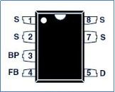
Pins Description of LNK304GN IC:
Pin Number | Pin Name | Description | |
01 | 1,2,7 & 8 | Source (S) | Ground reference for Bypass & Feedback pins and a power MOSFET source connection. |
02 | 5 | Drain (D) | Power MOSFET drain connection, provides internal operating current for start-up and steady-state operation |
03 | 3 | BYPASS (BP) | Connection point for a 0.1uF external bypass capacitor for internally generated 5.8 volts supply. |
04 | 4 | Feedback (FB) | For control of switching operation of power MOSFET during normal operation. |
Features of LNK304GN IC:
- It has a wide supply range of 85 VAC to 265 VAC.
- Low cost and energy efficient.
- Lowest component count.
- SMD manufactured.
- Drain Pin voltage: -0.3 to 700 V (at TA = 25 C).
- Drain Pin Peak current: 400 (750) mA. (Higher when VDS > 400V)
- Feedback Pin voltage: -0.3 to 9V (TA = 25 C)
- Feedback Pin Current: 100 mA. (TA = 25 C)
- BYPASS Pin Voltage: -0.3 to 9V (TA = 25 C)
- Operating Supply Current: 200 uA
- Duty Cycle Max: 72%
- ON Time Max: 475 ns
- Operating Junction Temperature: -40 C to 150 C
- Output Frequency Max: 70 KHz (TJ = 25 C)
- Output Voltage: 12V
- Output Current: 170 mA
Note:
- TA = Ambient Temperature
- TJ = Junction Temperature
- VDS = Drain to Source Voltages
LNK304GN Equivalent: LNK304GN-TL.
Alternative Off-line Switcher IC: LNK302P, LNK302DG.
Uses of LNK304GN:
LNK304GN has the features of low component count, low cost and extremely energy efficient IC which can be used to construct different topologies as per the demand. It can be used to support Buck, Buck-boost and flyback topologies. It has hardwired auto start circuit which is used for the protection of the circuit in case of short circuit and open loop faults. Keeping its features intact switching mode power supply could be designed without the use of transformer in it. With its higher performance it can be used in different appliances, timers, LED drivers and industrial controls. LNK304GN with combination of different electronic components could be utilized to obtain different topologies i.e. High-Side-Buck-Direct Feedback, High-Side-Buck-Optocoupler Feedback, Low-Side-Buck-Constant-Current LED Driver etc.
Working of LNK304GN:
From the internal circuit configuration of LNK304GN IC it has combined a high power MOSFET switch with a power supply controller all resides in one device. It uses simple On/Off control for output voltage regulation. The controller consists of oscillator which has an internal oscillating frequency of 66 KHz. Oscillator generates two signals i.e. the maximum duty cycle signal and clock signal which is for indication of the beginning of each cycle. To minimize EMI emission oscillator incorporates circuitry that introduces a typical value of 4 KHz frequency jitter. The modulation rate of the frequency jitter is kept 1 KHz in order to optimize EMI emission.
At the FEEDBACK pin it has feedback input circuit with low impedance source follower and output set to 1.65 V. Whenever the input current to this pin will exceed from 49 uA, a low level logic will generate at output of feedback circuit. At the rising of each cycle output of this signal is sampled at the very beginning if it is high the power MOSFET for this cycle will be ON otherwise it will remains OFF.
BYPASS capacitor is connected at the BYPASS pin and voltage regulator will charge this capacitor to 5.8 V, whenever the BYPASS pin voltages drop below 4.85 V power MOSFET will be disabled...
Read more »
 utsourceproduct