0%
0%
Yet another guide on how to make PCBs at home
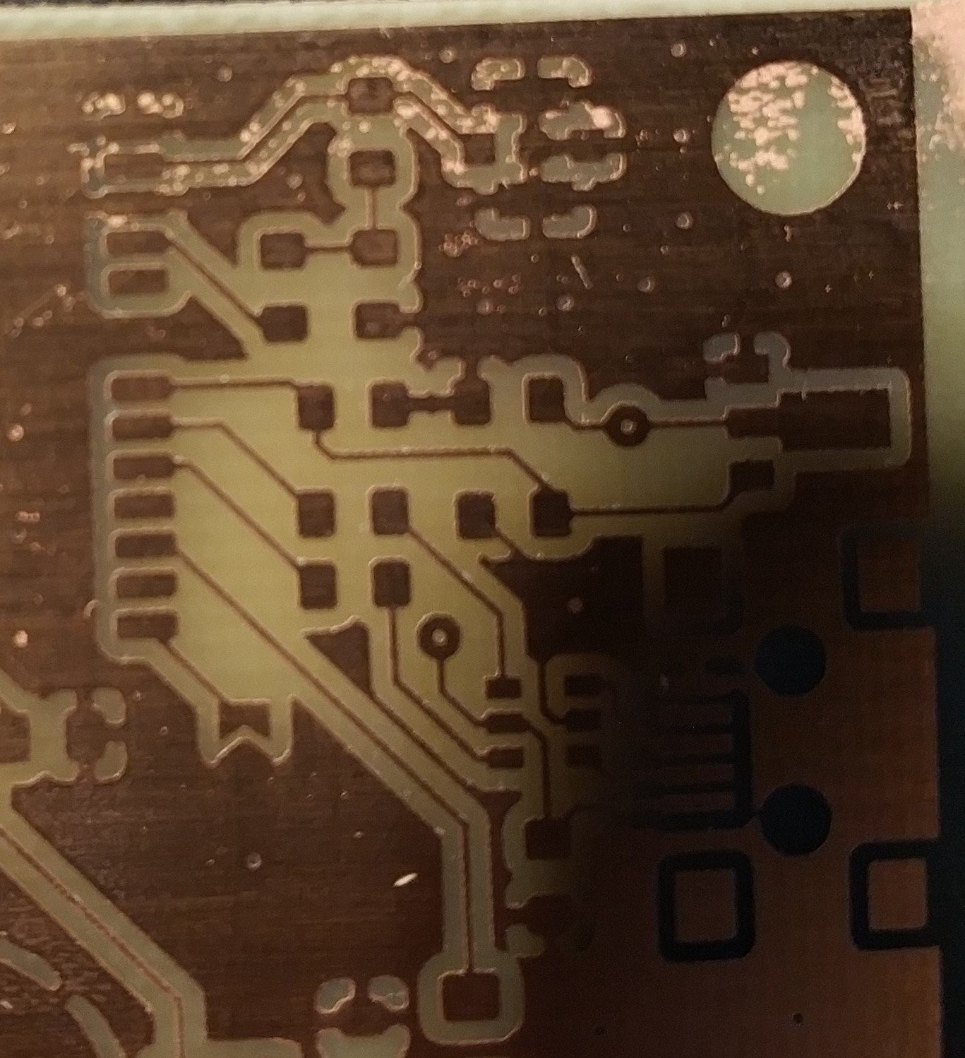
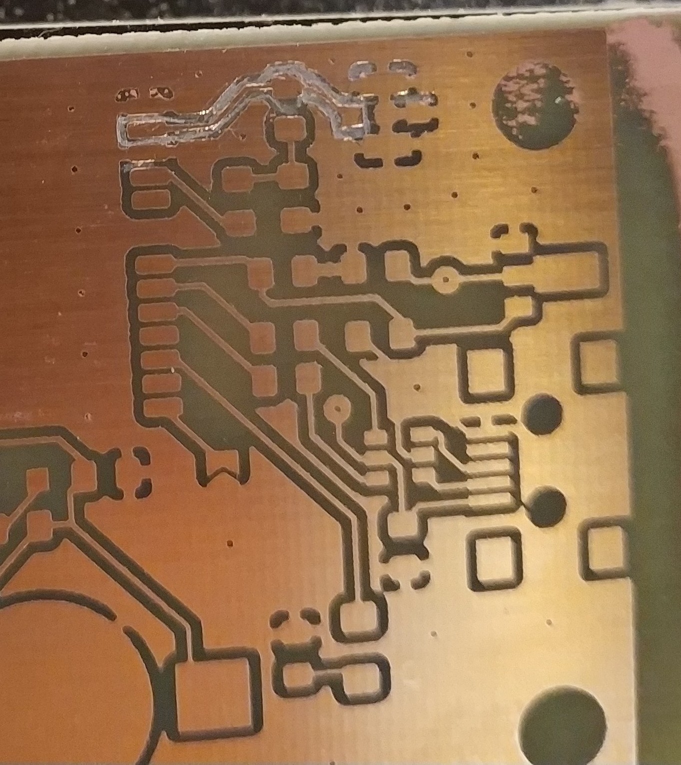
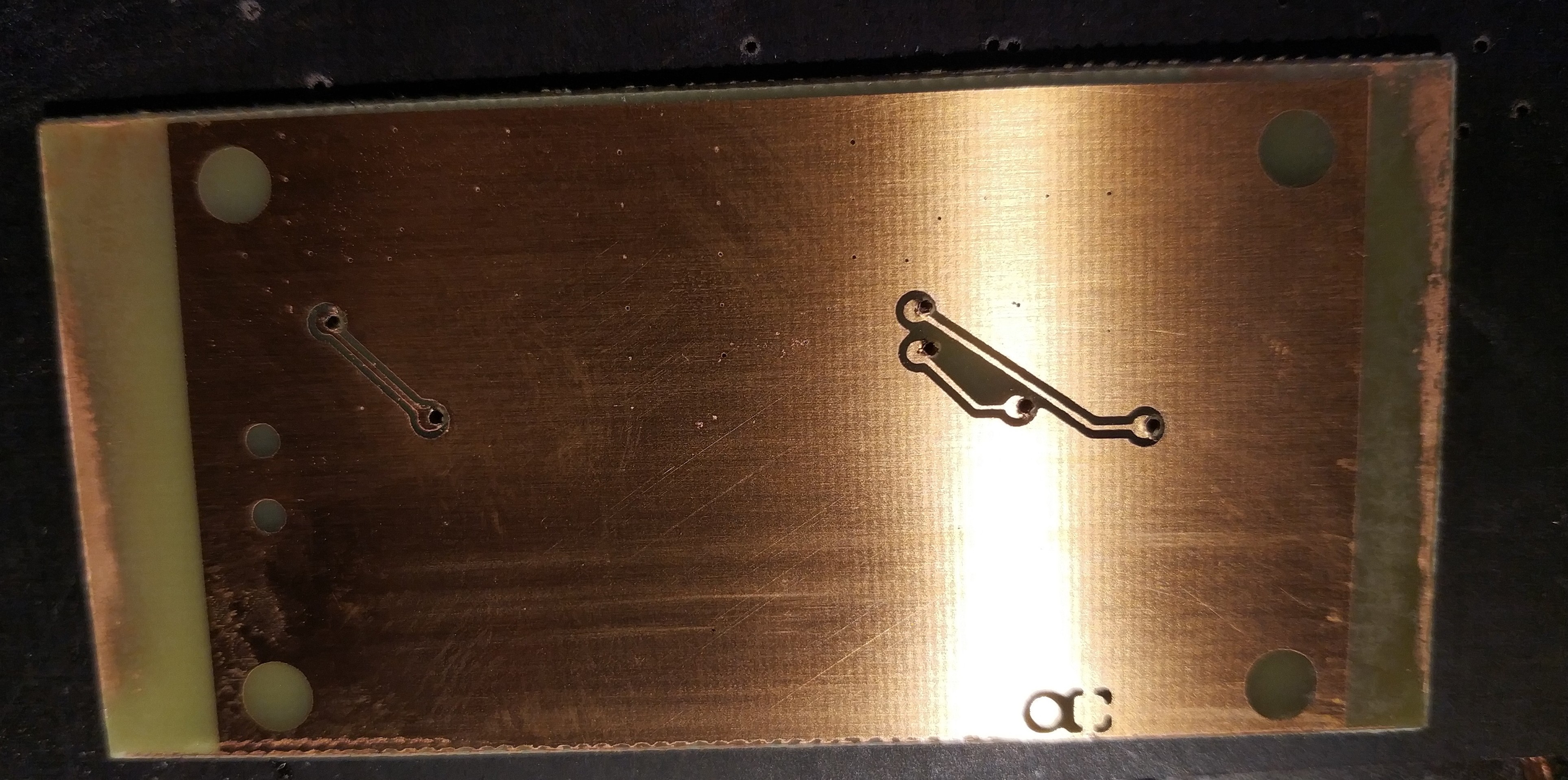
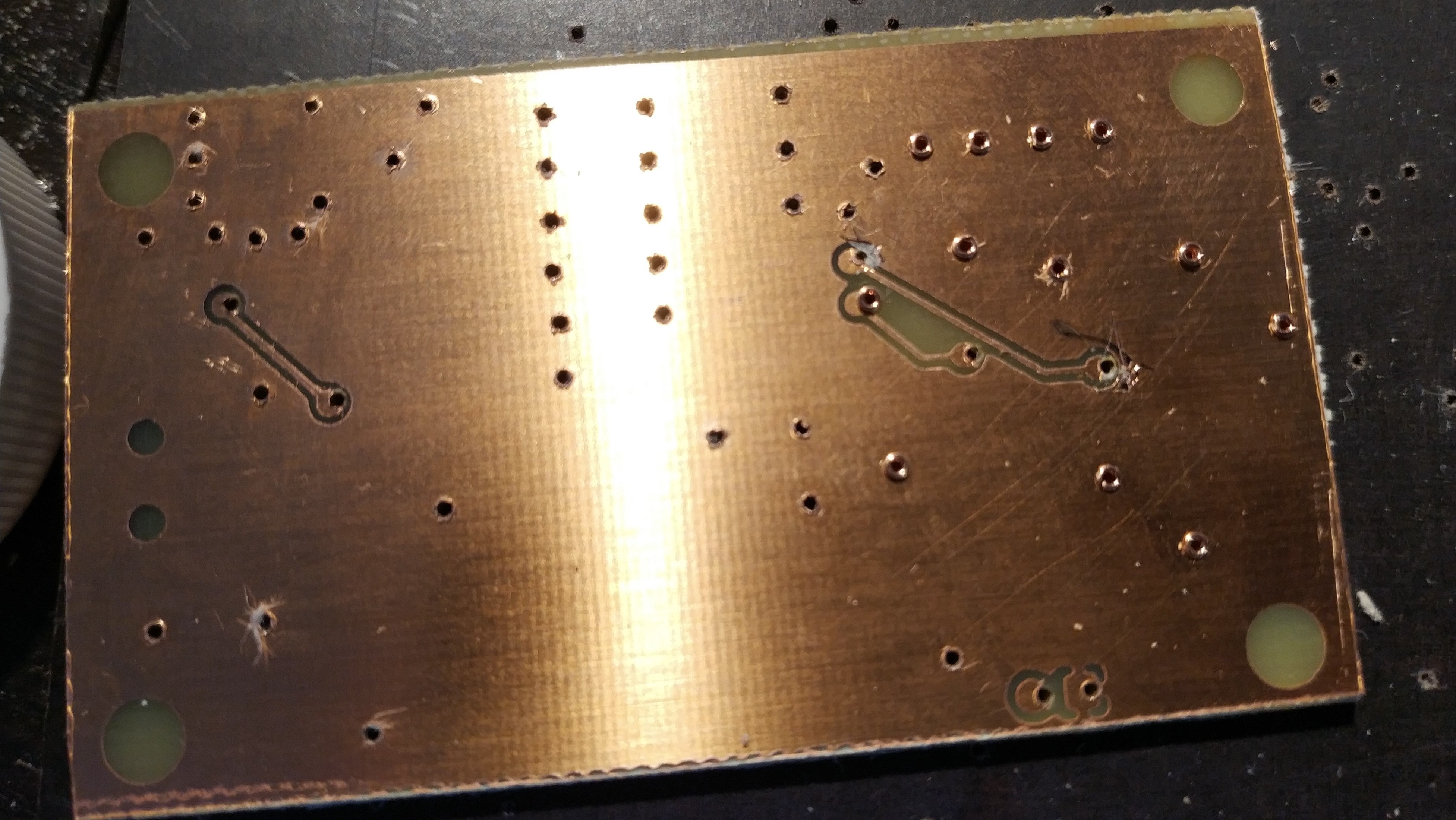
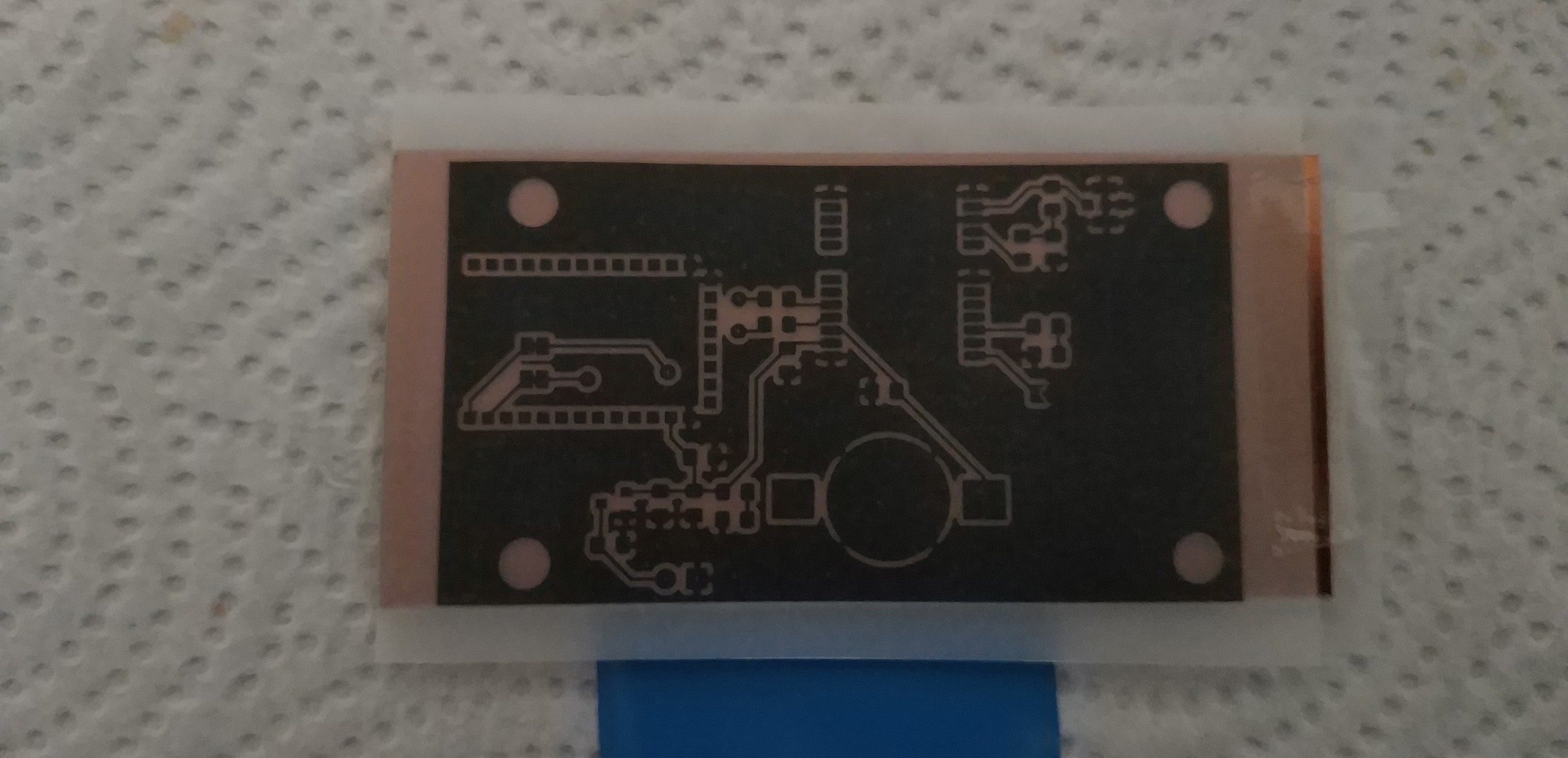
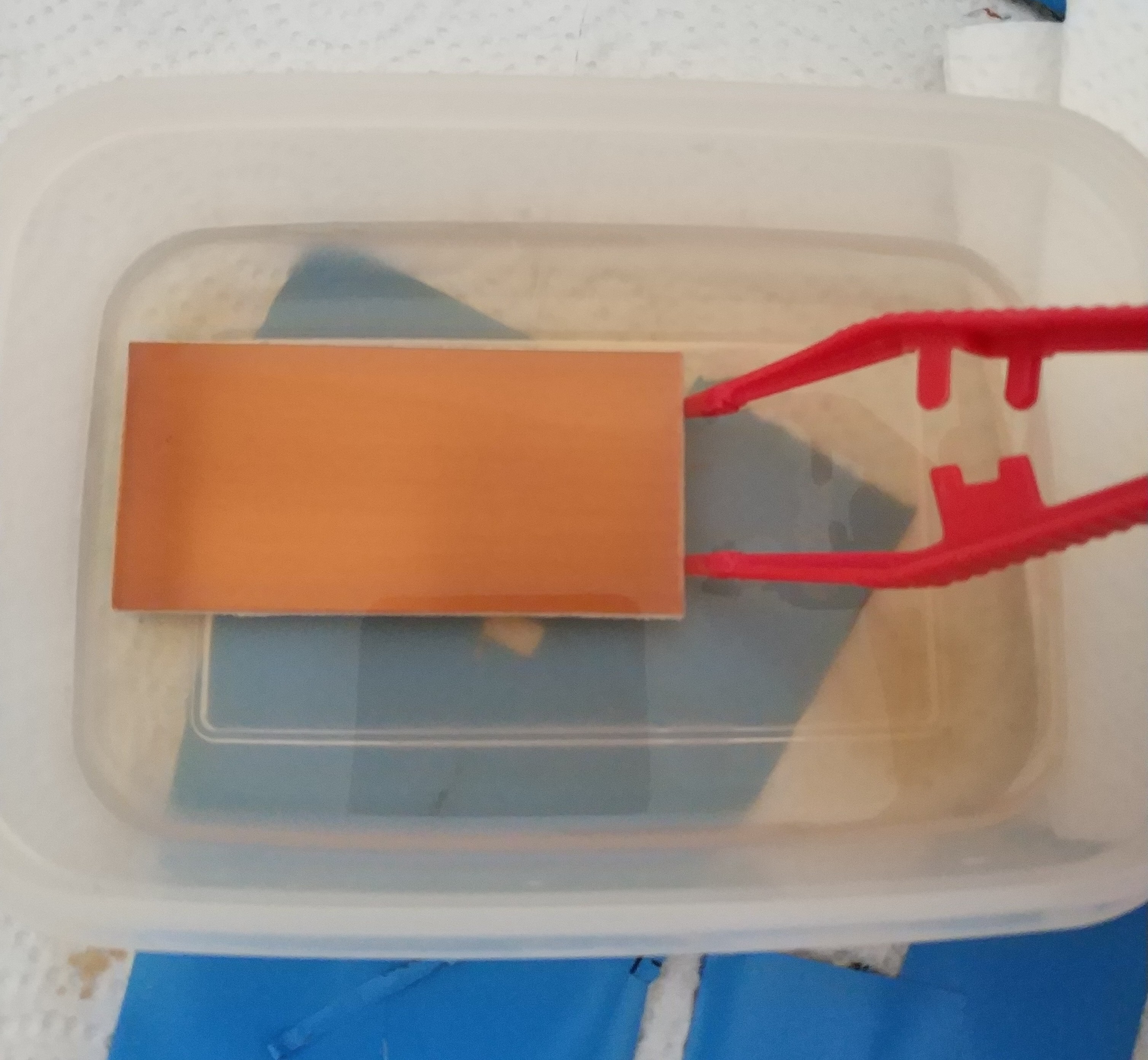
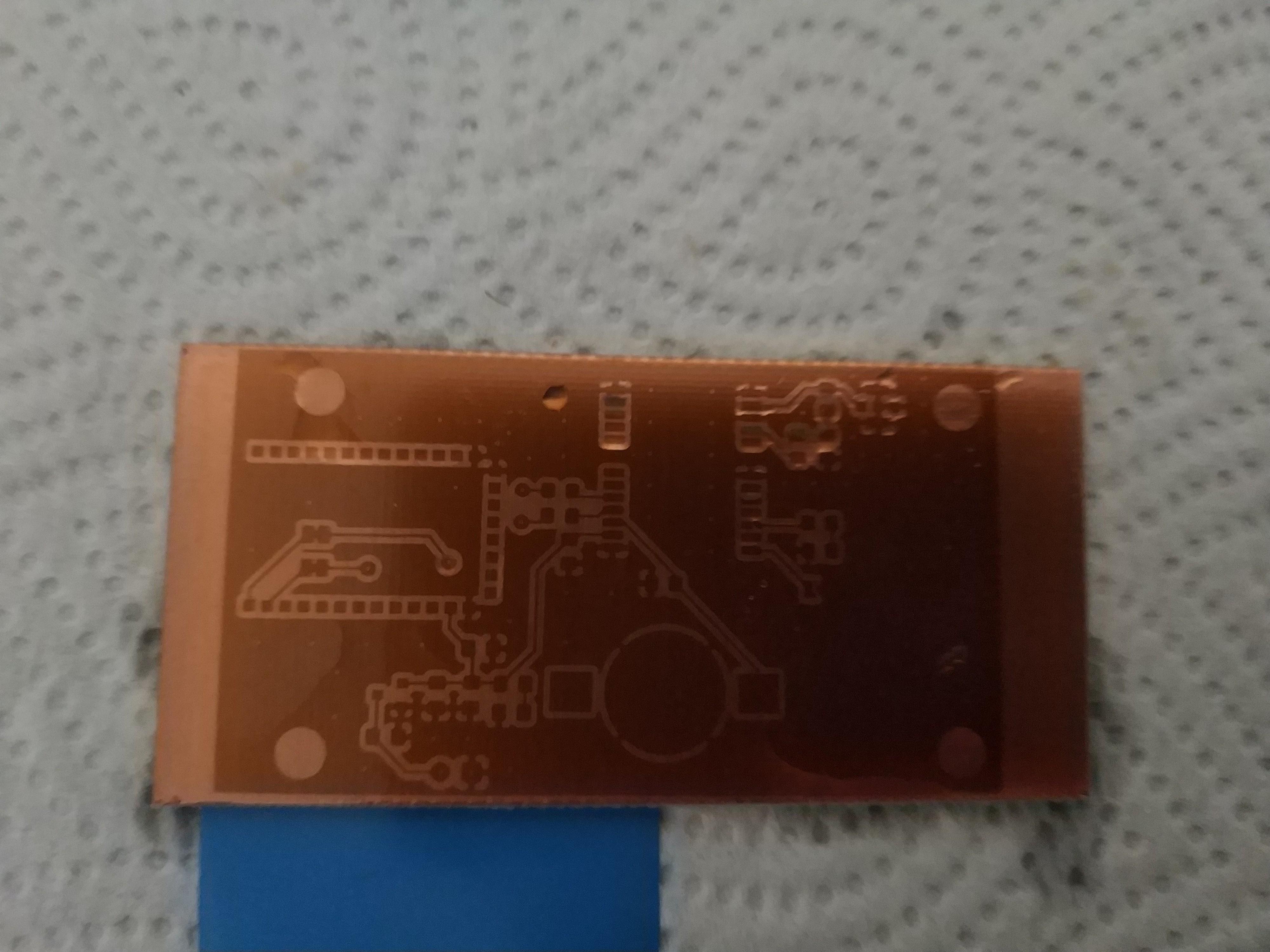
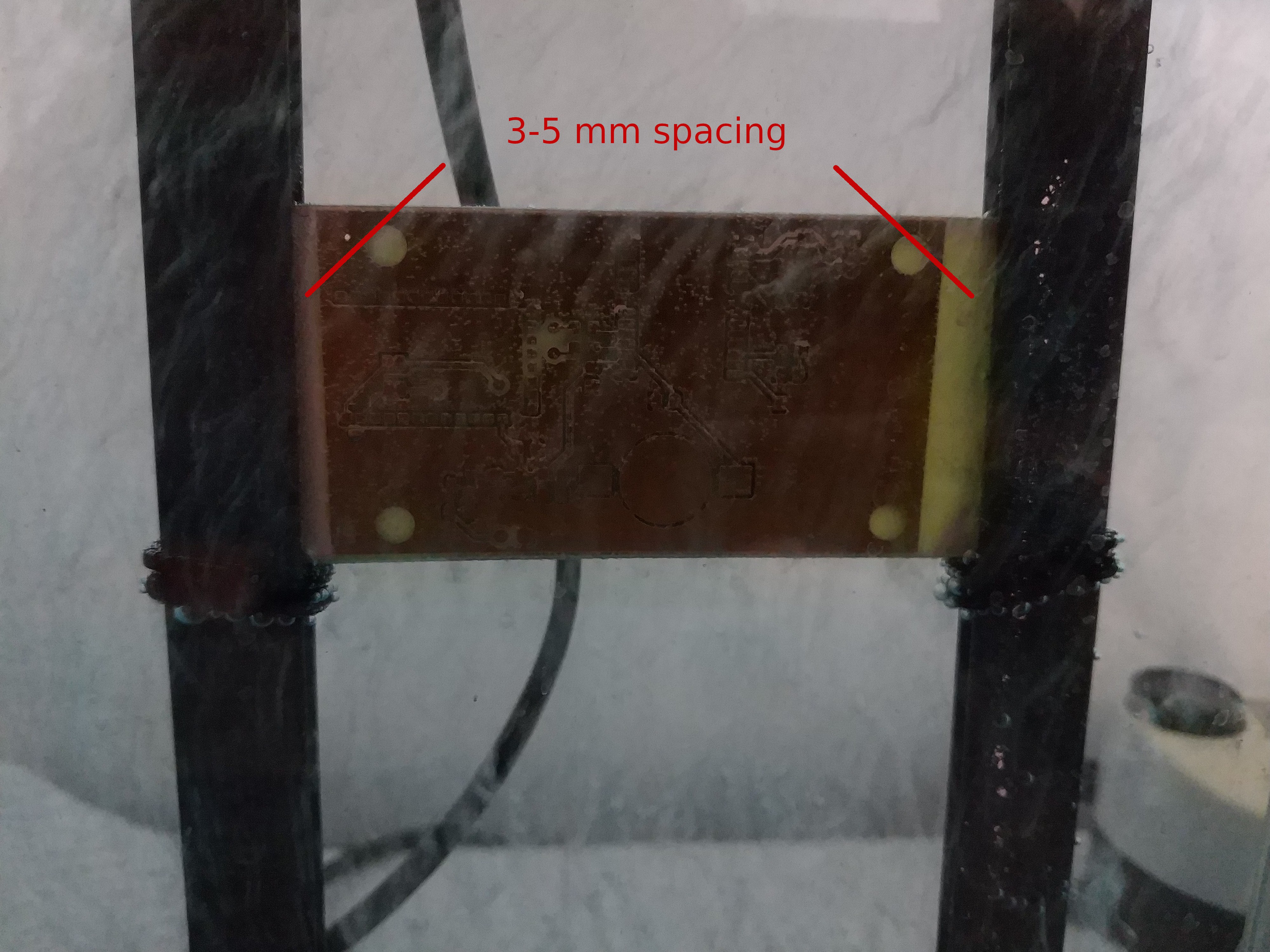
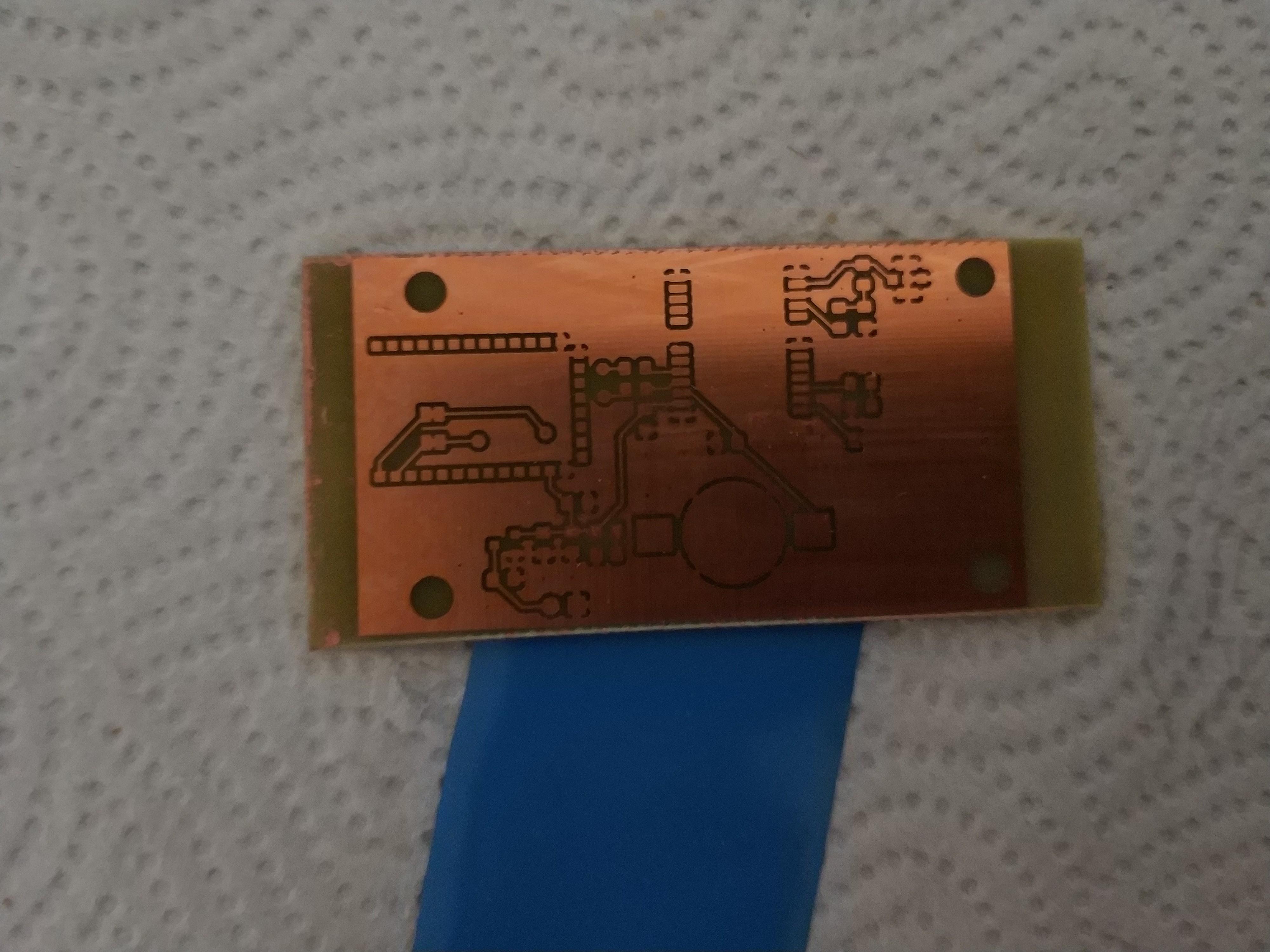
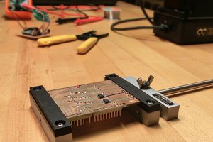
Here I describe my method for making 1 and 2 layer PCBs at home via lithography and etching
Become a Hackaday.io member
Already have an account? Log in.
Just one more thing
To make the experience fit your profile, pick a username and tell us what interests you.
Pick an awesome username
hackaday.io/
Your profile's URL: hackaday.io/username. Max 25 alphanumeric characters.
Pick a few interests
Projects that share your interests
People that share your interests
 Alex Rich
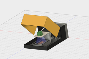
 Jonathan Beri
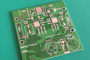
 Marius Taciuc
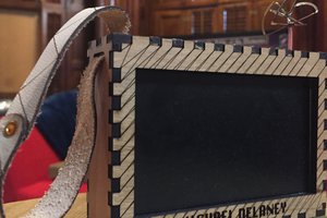
 Michael Delaney