 Leonardo Ward
The electronic design for the Onboard Gateway will contain the following main components:
- ESP32 DEVKITC 32D
- RFM95W (LoRa)
- USB LiIon LiPoly Charger Board (3.7V 1 Cell Battery Charger)
Once we selected the main components we created a schematic and designed the PCB.
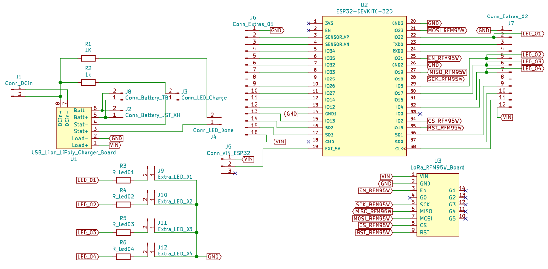
Schematic
Bill Of Materials
| Quantity | Name | Description |
| 1 | RFM95W LoRa Radio | LoRa Module |
| 1 | ESP32-DEVKITC-32D | ESP32 Module |
| 1 | USB LiIon/LiPoly charger | 1 Cell 3.7V Battery Charger |
| 2 | TERM BLK 2P SIDE ENT 5.08MM PCB | Battery Connector, and External Power Source |
| 1 | CONN HEADER R/A 2POS 2.5MM | Battery Connector |
| 2 | CONN HEADER VERT 40POS 2.54MM | Male Headers |
| 1 | CONN HDR 2POS 0.1 GOLD PCB | Connector for the Battery Charger |
| 1 | CONN HDR 3POS 0.1 GOLD PCB | Connector for the Vin Selector (5V or USB for the ESP32) |
| 1 | CONN HDR 5POS 0.1 GOLD PCB | Connector for the LoRa Module |
| 1 | CONN HDR 6POS 0.1 TIN PCB | Connector for the Battery Charger |
| 1 | CONN HDR 9POS 0.1 GOLD PCB | Connector for the LoRa Module |
| 2 | CONN HDR 19POS 0.1 TIN PCB | Connector for the ESP32 |
| 1 | CONN JUMPER SHORTING .100" GOLD | Vin selector for the ESP32 |
| 1 | GPS Antenna | GPS Antenna |
| 2 | LoRa and GSM Antenna | LoRa and GSM Antenna |
| 1 | CONN HDR 16POS 0.1 TIN PCB | Connector for the ESP32 (to use the other available pins) |
| 1 | CONN HDR 12POS 0.079 GOLD PCB | Connector for the ESP32 (to use the other available pins) |
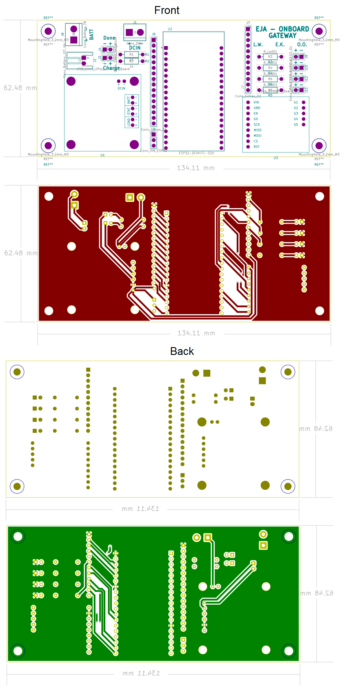
PCB Layout
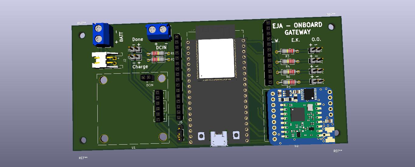
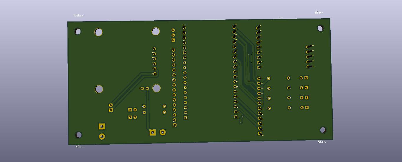
3D Model
Discussions
Become a Hackaday.io Member
Create an account to leave a comment. Already have an account? Log In.