 Sam Griffen
Today was the second successful test for Chad. I have been working on an anemometer for this project, and needed to have a PCB for the control board. For more detail on the actual board, I have an upcoming project log in that other project. Here I just want to talk about the milling results, and how I got them. First up, heres the board:
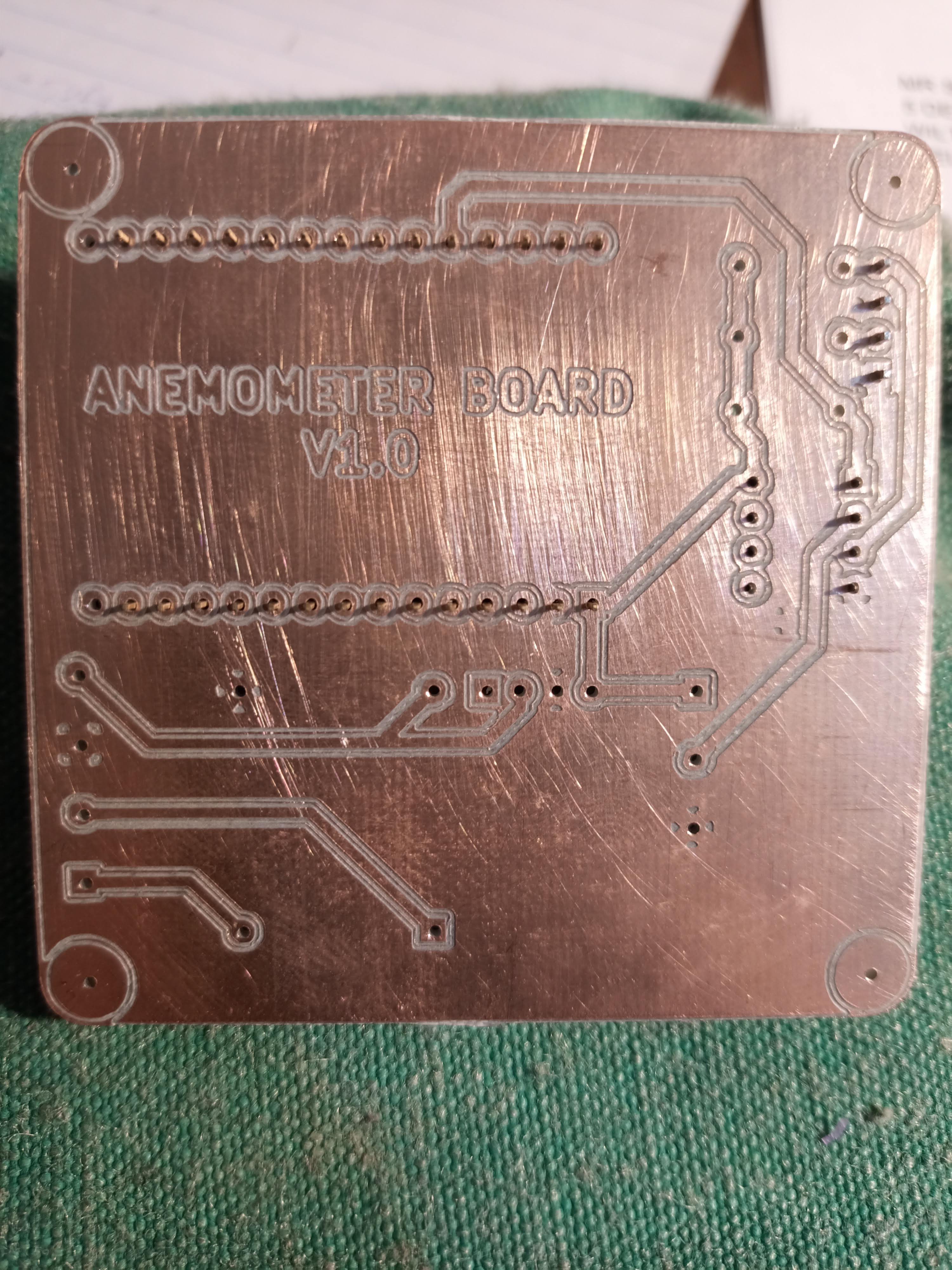
I have given it a .... light .... sand (Note to self, use finer paper next time) to get rid of some nasty burrs and whatnot. There is an annoying interaction between the ground pour and the traces, causing an annoying area of copper between the trace and the plane. I think this could potentially be remedied by reducing the clearance between the ground pour in KiCAD and the traces?
When milling the actual traces, I definitely went too deep into the copper. I had problems with the first attempt, with the bit not breaking the surface of the copper, so swapped in some fresh copper and increased the Z cut distance. I ended up cutting in about 1.05mm, as a multi depth cut. By about 0.09mm the copper was well and truly isolated, which is what the original forum post I read about FlatCAM recommended. In future I will cut shallower, and possibly do a second run over with a deeper cut distance if there are issues.
Drilling has all been done at 0.8mm, however some holes need to be wider than this. I plan to just go in with a hand drill to make these holes bigger. Possibly in future I could mill the mounting holes? However this seemed scary, and I have opted to steer clear of that for now.
Cutting out the board was a real pain. Because I really wanted the nice round corners, I had to edit export the cut layer from KiCAD, and process it as a seperate job in FlatCAM. Once processed into a FlatCAM geometry object, I had to use the edit tool to delete the inner path. While in the edit tool, I also drew a rectangle overlapping the cutout path, and used the cut path tool to essentially create fingers to hold the board in place.
I guess it wasn't too bad after this, I just needed to process the geometry into a CNC job. I have a 1.6mm endmill that does a really good job at board cutouts. The only issue here was that I again went too deep. 2.1mm is far more than the PCB, and I should just stick to about 1.8mm, that seems to get through the entire board quite easily.
The main takeaways from this board are that I should trust myself, and go for shallower cuts into the copper, and into the board in general. Also, I really need to get some sort of vacuum to get rid of all the dust as Chad works, to both clean up the outcome, and to make sure I'm not inhaling bad things left and right.
If anybody reading this has any pointers on things I can do differently, I'd love to hear it!
Discussions
Become a Hackaday.io Member
Create an account to leave a comment. Already have an account? Log In.