 Said Alvarado Marin
Designing a 4x4cm PCB for LEDs that are supposed to handle up to 26Watts of power is not a trivial task. In this log we are going to take a look into the design process.
Most of the information and images from this log are taken directly from this amazing application note:
Optimizing PCB Thermal Performance for Cree® XLamp® LEDs
If you need to design PCBs for high power LEDs, this is where you should start. The application note is filled with thermal simulations and tests to figure out the cheapest and most efficient way of drawing heat away from your LEDs
Now then, the PCB we are going to be taking a look at is the following one:
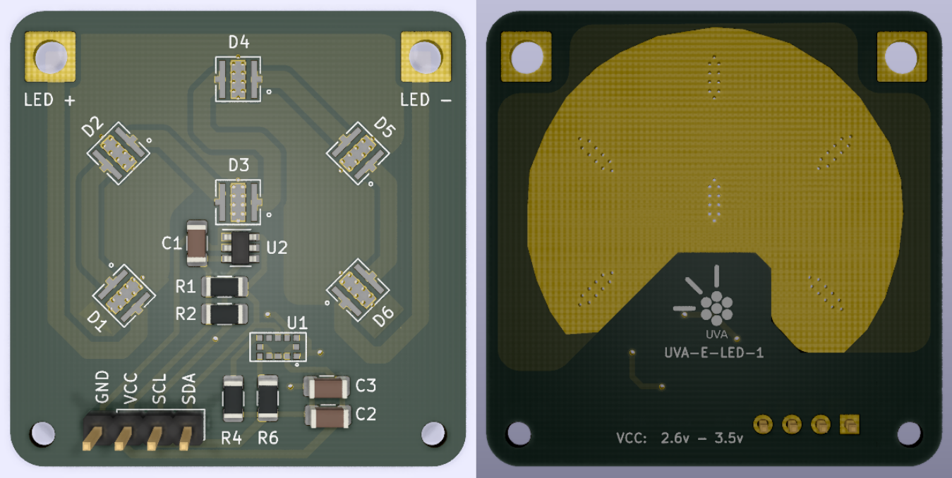
It is supposed to hold 6 5Watts ultra violet LEDs, as well a couple of sensors on the front. And on the back have space for a big Heatsink.
The goal
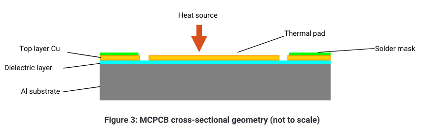
The main purpose of this PCB is to efficiently transmit heat away from the LED and into the Heatsink. This way we avoid over-heating and damaging the PCBs. The gold standard for this are MCPCB. Which (unlike most PCBs) are mostly made from aluminum to maximize their thermal conductivity.
Summary the Cree's Application Note
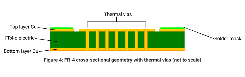
The Application note proposes that it is possible to dramatically increase the thermal conductivity of a FR4 PCB by making it very thin and adding a ton of thermal vias, like in the following diagram:
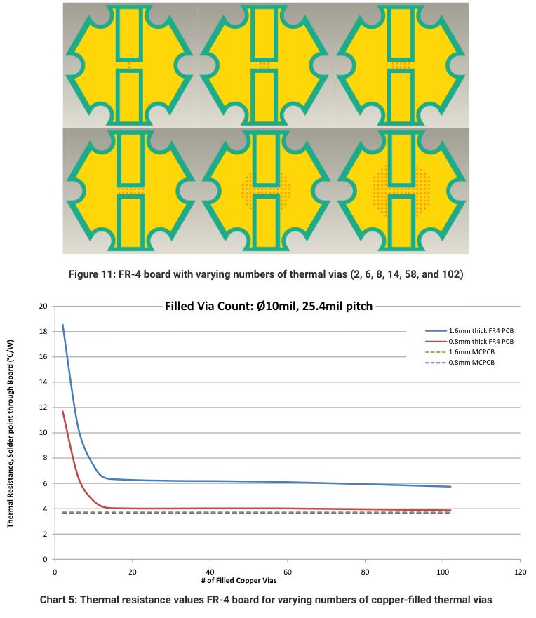
The document has a bunch of really cool simulations where they test several different factors of the PCB. Like for example the following where they validate that thermal vias are useful, but only really worth it if they are directly below the LED.
Of all the factors discussed and taken into consideration. I used took away the following 4 for my design
Most important considerations
- The thinner the PCB the better. 0.8mm thick gives good results
- The thermal vias should be as small as possible. They use and recommend 0.25mm diameter
- Place as many vias below the LED's thermal pad as you can.
- Maximize the copper area in contact with the Thermal vias both at the front and at the back of the board.
- If it's possible to fill the thermal vias with solder while you're assembling the PCB, good. That also helps.
Implementing the recommendations
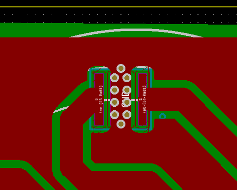
Let's concentrate on the footprint of a single LED.
- The vias had to be 0.3mm in diameter because that's the smallest the PCB manufacturer would allow
- A total of 10 vias fitted right below the Led
- Both front and back the thermal pad is connected to large copper planes
- The PCB was manufactured at 0.8mm tick instead of the more standard 1.6mm
It is laborious work to set everything up like that. But the results were good with this configuration.
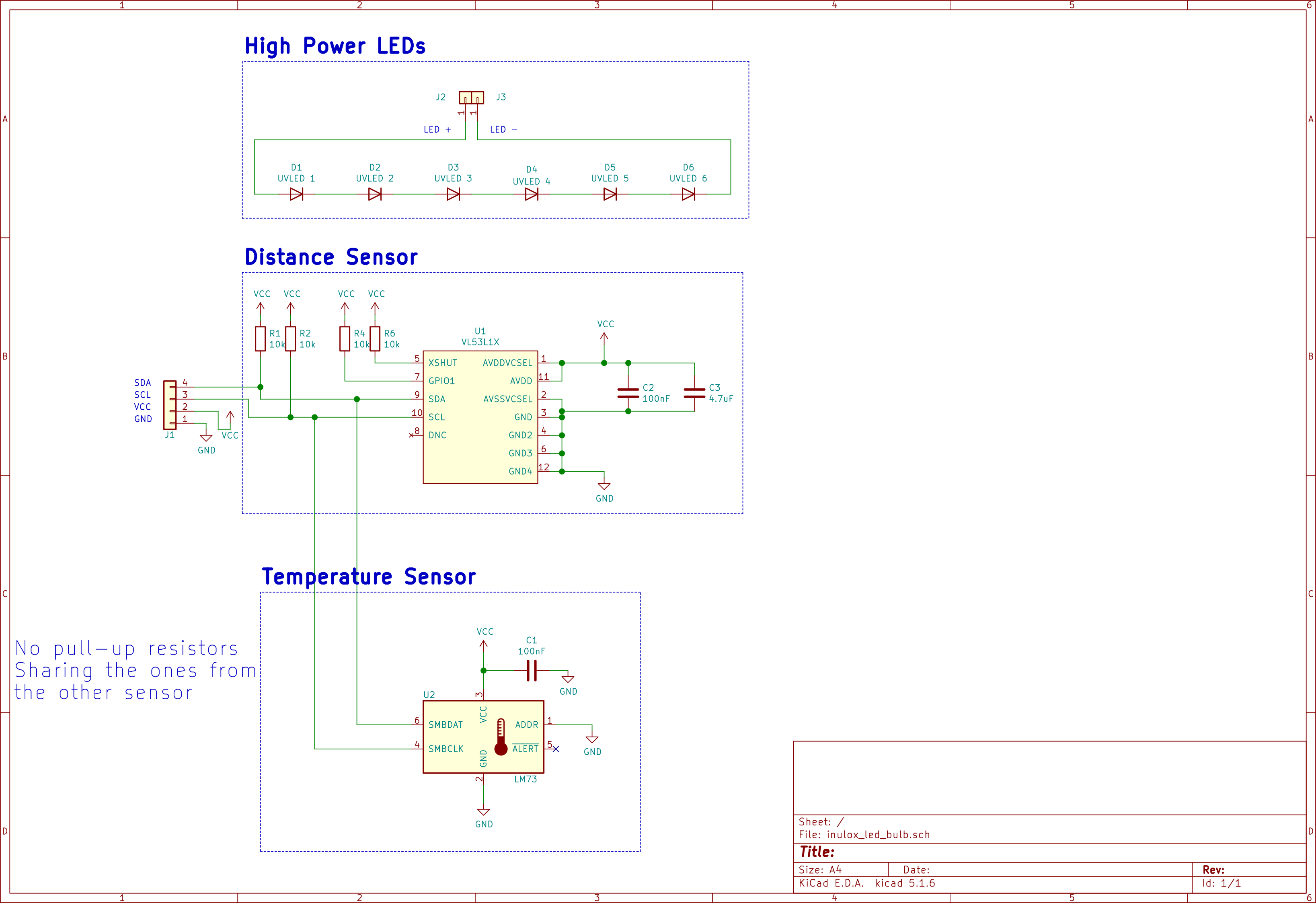
A word on the schematics
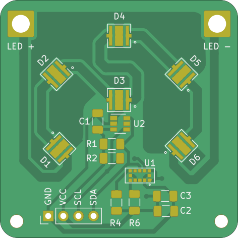
This PCB also houses a couple of sensors, namely U1 and U2:
Temperature Sensor - LM73
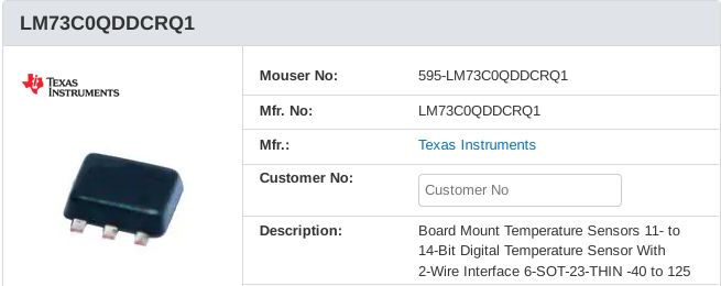
This is a small I2C digital temperature sensor from Texas Instruments. It helps monitor the temperature of the LEDs to make sure they are not overheating. It was chosen mostly because it was the only small I2C temperature sensor, with good library support and in a NON-QFN package (to simplify soldering.) that I could find.
It was installed as closed to the LEDs as possible. And It's ground pin was connected to the LED's Thermal plane, to improve thermal transference between the LED and the sensor.
Distance Sensor - VL53L1CX
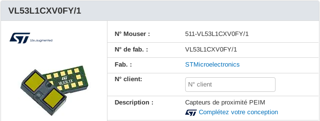
We would also like to monitor the distance from the LED to the closest surface. So we chose a small distance sensor to accomplish this task. Since the Flashlight has to operate in an environment of high luminous intensity, be it outdoors or on it's own High power UV reflections, all reflective-based sensor were disqualified. Which is why we chose with this Time-of-flight sensor. Which is conveniently controlled through I2C. Sadly it comes in a QFN package, but there is not much we can do about that.
It was installed far away from all the heat generating components.
Full schematics
The schematics of both sensors are very straight forward. They only need a handful of capacitors and resistors, which the datasheet points of how to select. The final schematics for the PCB is the following:
Discussions
Become a Hackaday.io Member
Create an account to leave a comment. Already have an account? Log In.