 engineerkid1
Metal Oxide Semiconductor Field Effect Transistor (MOSFET) is voltage controlled device which like bipolar junction transistor can be used for amplification and switching of electrical signals. since they are manufactured by oxidation of semiconductor especially silicon hence also called MOS transistors. It is a three terminal device with terminals called Gate, Drain and Source. Voltage applied at the gate terminal are used to control the operation of the device
FTP11N08A is a N channel MOSFET, N channel MOSFETs has a N type conducting region between drain and source. This deice has low drain source ON resistance, low leakage current and high forwarded transfer admittance.
Features of FTP11N08A
- RoHS Compliant
- Low ON Resistance
- Low Gate Charge
- Peak Current vs Pulse Width Curve
- Inductive Switching Curves
Replacement Part
AOT2500L/ AOB2500L
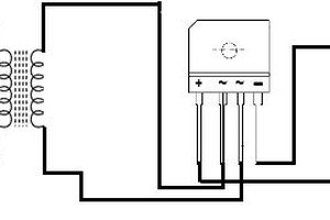
Pictorial View
Pictorial view of the N-Channel MOSFET is shown in figure below, it is available in TO-220 package

Pin Description
Pin diagram and pin description of the FTP11N08A is given below

Pin Number | Pin Name | Description |
1 | G | Gate |
2 | D | Drain |
3 | S | Source |
IC Electrical Characteristics/ Specifications
Some Electrical characteristic of the device are given below
Parameter | Description | Value |
VDSS | Drain to source voltage | 75 V |
ID | Continuous drain current | 100 A |
ID AT 100 C | Continuous drain current at 100 C | 70 A |
IDM | Pulsed drain current | 100 A |
PD | Power dissipation | 230 W |
VGS | Gate to source voltage | -20 to 20 V |
EAS | Single pulse avalanche energy | 600 mJ |
TJ | Junction temperature | -55 to 175 C |
TSTG | Storage temperature | -55 to 175 C |
Ciss | Input capacitance | 4541 pF |
Coss | Output capacitance | 717 pF |
Working Principle
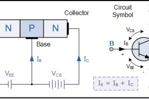
N channel MOSFETs has N channel between the Drain and Source terminal and P type substrate Current flows due to negative charge carriers in this type of devices. Since these are voltage controlled devices and control voltages are applied at the gate terminal of device, very little or no current flows through the gate. When positive voltages are applied at the gate terminal it pushes the positive charge carries into the substrate and attracts the negative charge carries into the N channel thus increasing its conduction.
Applications
UTsource FTP11N08A is recommended for following applications
- Automotive
- DC motor control
- Class D amplifier
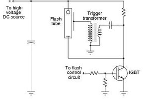
Motor control Circuit
DC motor control circuit for bidirectional and speed control is shown in circuit diagram below, two N channel and two P channel MOSFET are utilized in the circuit. Gate of the MOSFTs can be derived from some microcontroller or manually.

Class D Amplifier
Class D amplifier is also called switching amplifier in with the active device functions as a switch, they switch back and forth between the positive and negative supply rails according to input pulses.

 kamalkedin123
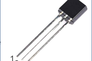
 Electroniclovers123