 zpekic
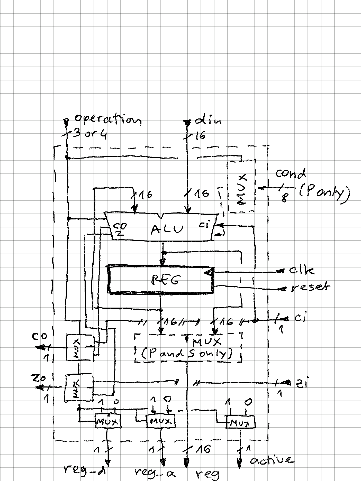
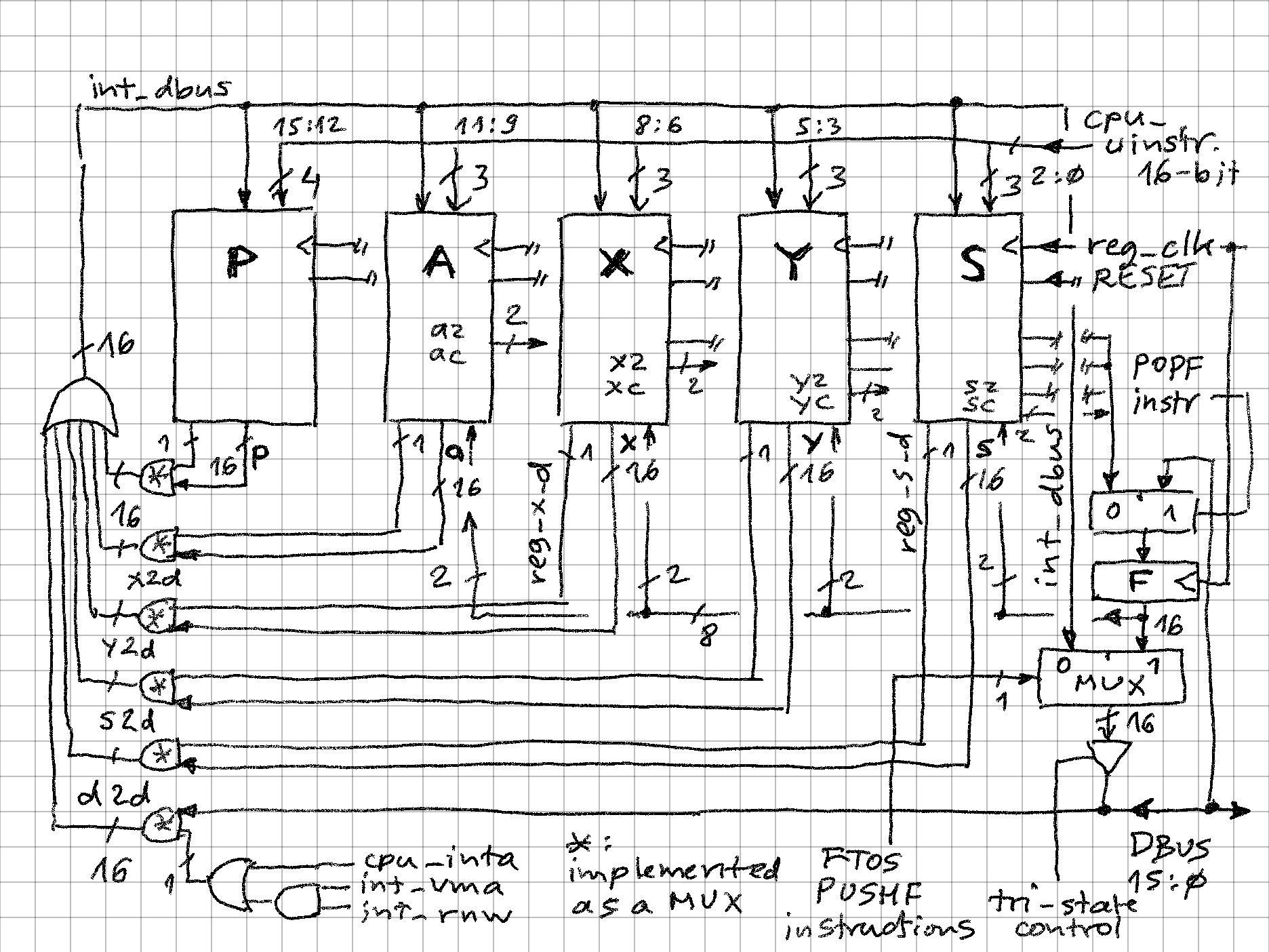
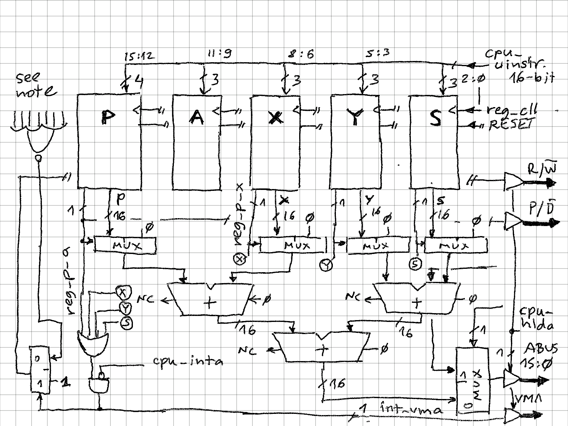
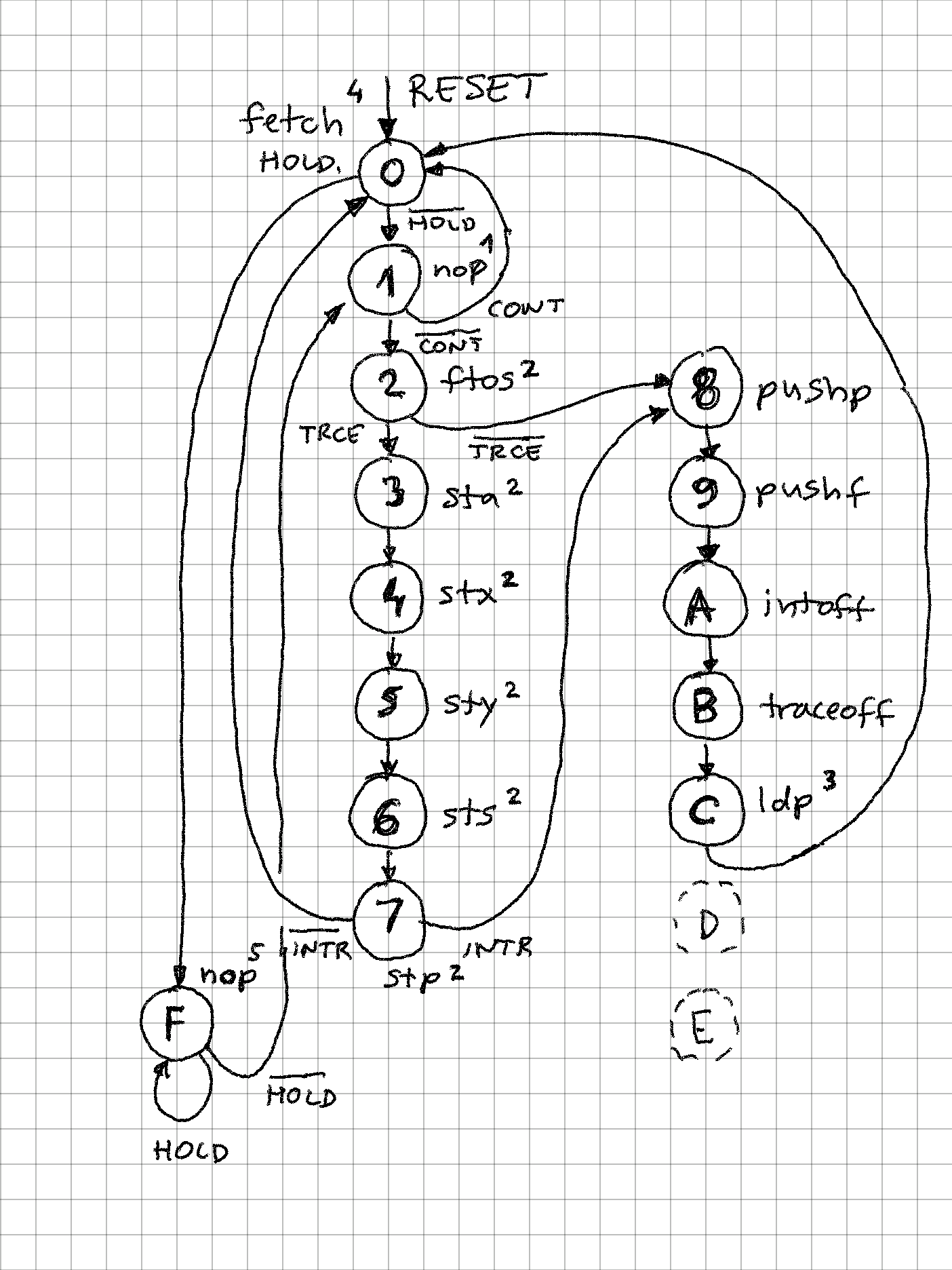
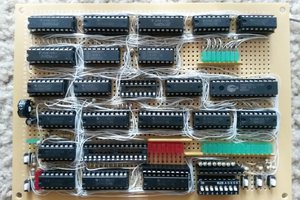
This is my main project now, and I am exploring the opposite of end of spectrum from my serial processor - while serial CPU processed with 1 bit a time, here there will be intrinsic parallelism, as each instruction could theoretically update 5*n bits (n = 16 in this implementation). Currently, the little test code I have is able to achive about 1.25 operations per instruction. I built in runtime counters that count instructions per second and operations per second. The max clock speed is 25MHz (12.5MIPS), probably with some tweaks full 50MHz could be achieved.
0%
0%
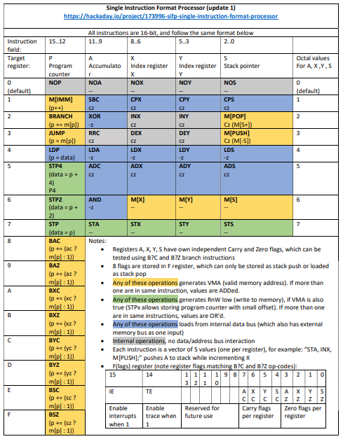
SIFP - Single Instruction Format Processor
A super-scalar, reduced instruction set processor where microcode and machine code are the same thing!
Become a Hackaday.io member
Already have an account? Log in.
Just one more thing
To make the experience fit your profile, pick a username and tell us what interests you.
Pick an awesome username
hackaday.io/
Your profile's URL: hackaday.io/username. Max 25 alphanumeric characters.
Pick a few interests
Projects that share your interests
People that share your interests


 ammarbhayat28
 Tim Ryan
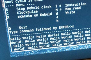
 Szoftveres
Hi Zoltan, I keep meaning to give you a 👍 but keep forgetting. I like that you are exploring non-traditional architectures. Someday I might get a round tuit to read your project in depth, and take the wrapping off the FPGA dev board I got some time back. In fact I need lots of round tuits. Have a great holiday season!