 marble
The biggest problem with the Colorlight is that all signals going to the HUB75 are going through 74HC245 octal bus transceiver, which direction pins are hardware to configure them as output.
Sadly, lifting the direction pin and configuring the transceivers as input would damage the FPGA with 5V, as discussed here. One could also lift the power supply pin of the IC and supply 3.3V instead of 5, but that would turn a whole bank of FPGA pins into input-only pins, which IMO defies the versatility of an FPGA.

My current approach is to de-solder the transceiver ICs and replacing them with bridge. The bridge is simply a PCB that connects each input to its corresponding output.
Ideally the boards would simply be castellated holes and traces connecting each input to its corresponding output.
I'm not the first one having ytrouble at this point. The problem is that the pitch of the tranceiver IC is so fine that no fab would accept the design. My guess is that the router bit would simply rip out the plating of the castellated holes if the drill diameter is too tiny.
Due to this problem I had to go through some design iterations until I arrived a something that was accepted by the fab.
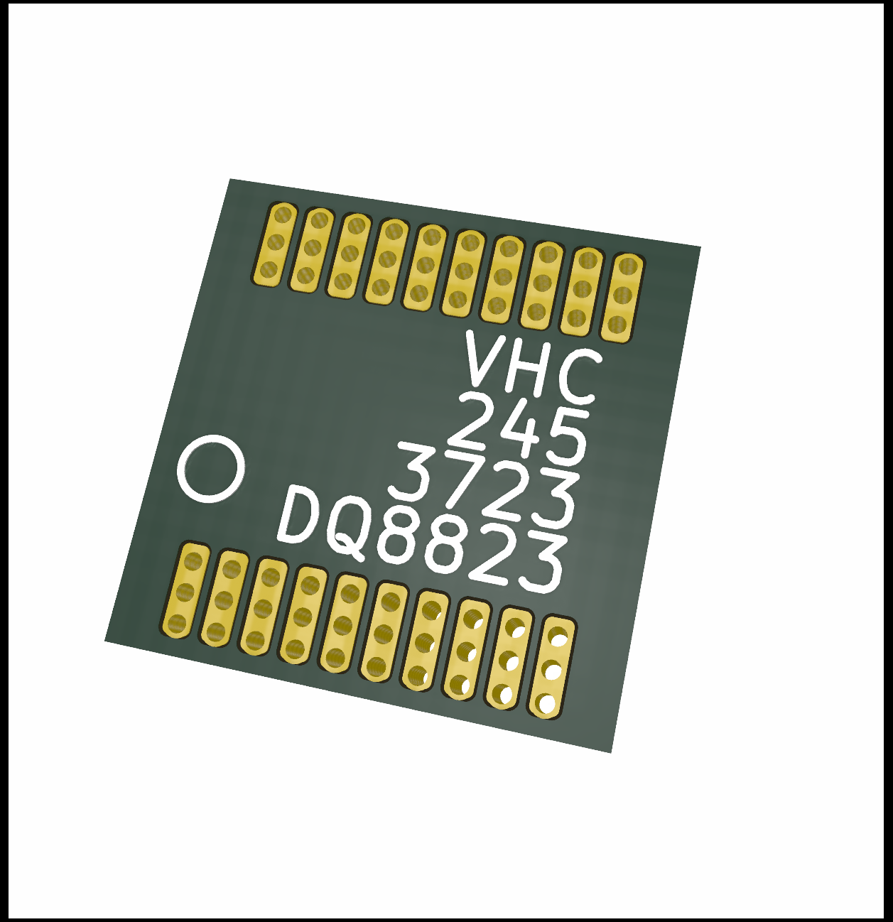
This design is essentially the footprint of the transceiver IC with the aforementioned traces, and holes through the pads.
The holes on one hand server the purpose wicking up excess solder, but also help aligning the PCB with the footprint on the Colorlight.

Discussions
Become a Hackaday.io Member
Create an account to leave a comment. Already have an account? Log In.