 Aditya Mukherjee
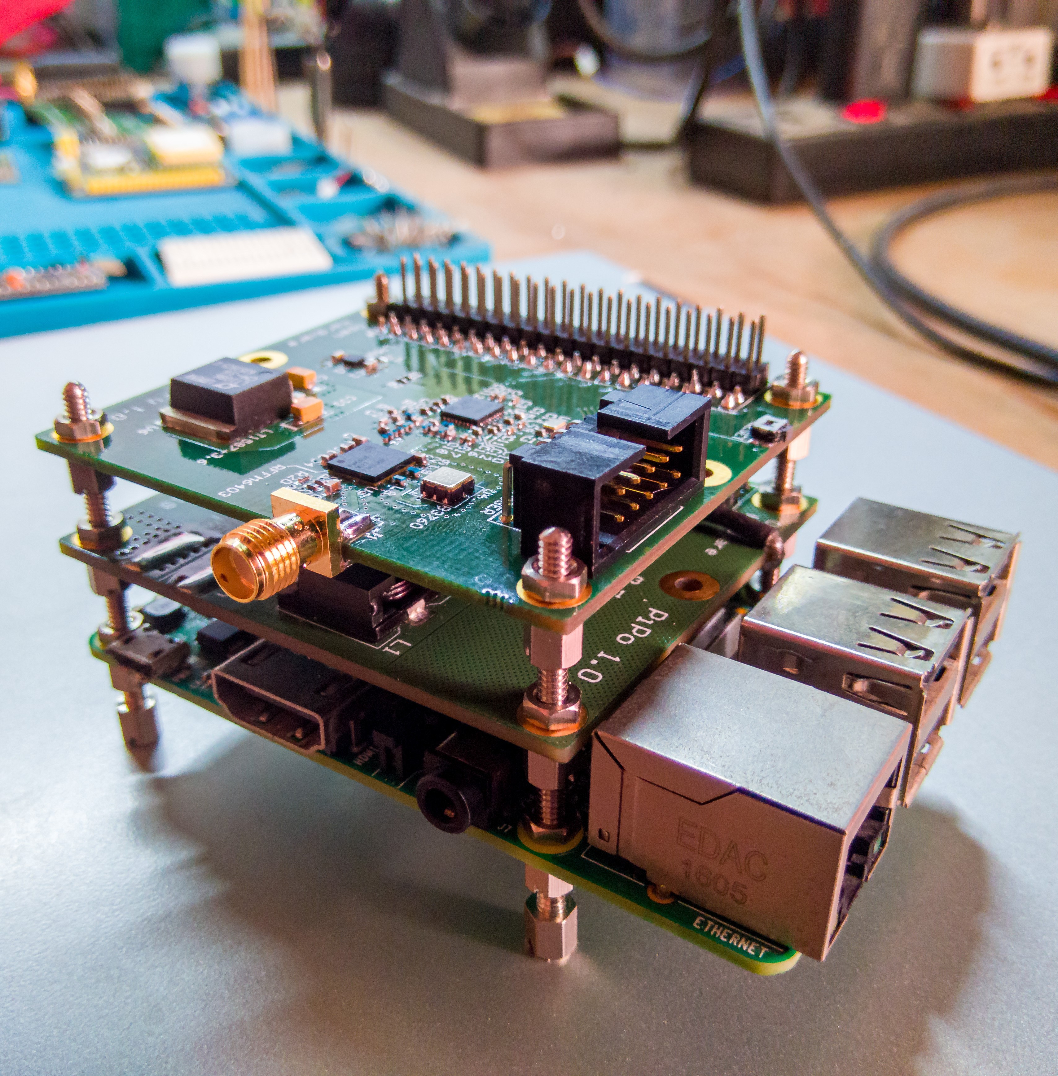
1. Power Delivery Board (PiPo):
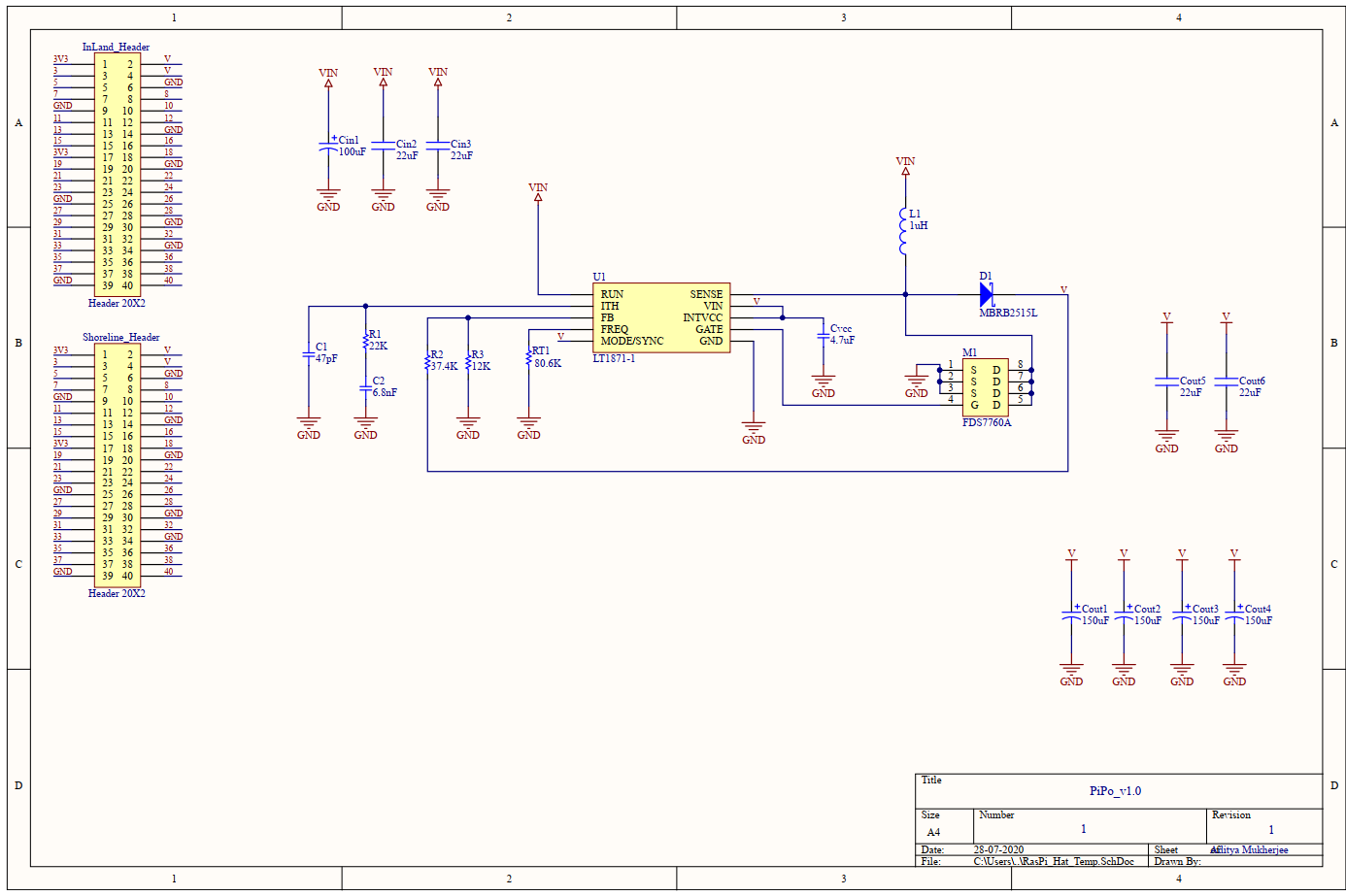
To run the essential hardware stacks a power delivery system more capable than a Raspberry Pi's internal power distribution was required. A design of a power distribution stack which could supply a high enough current with stability was adopted. The board was powered with a 3.7V LiIon or LiPo cell, its output was a constant 5V with a maximum allowed current of 7A. Our required peak current was 5A so, a 2A headroom was kept. The design was built around the LTC1871-1 - a wide input range, current mode, boost, flyback or SEPIC controller that drives an N-channel power MOSFET and requires very few external components.
Schematic:
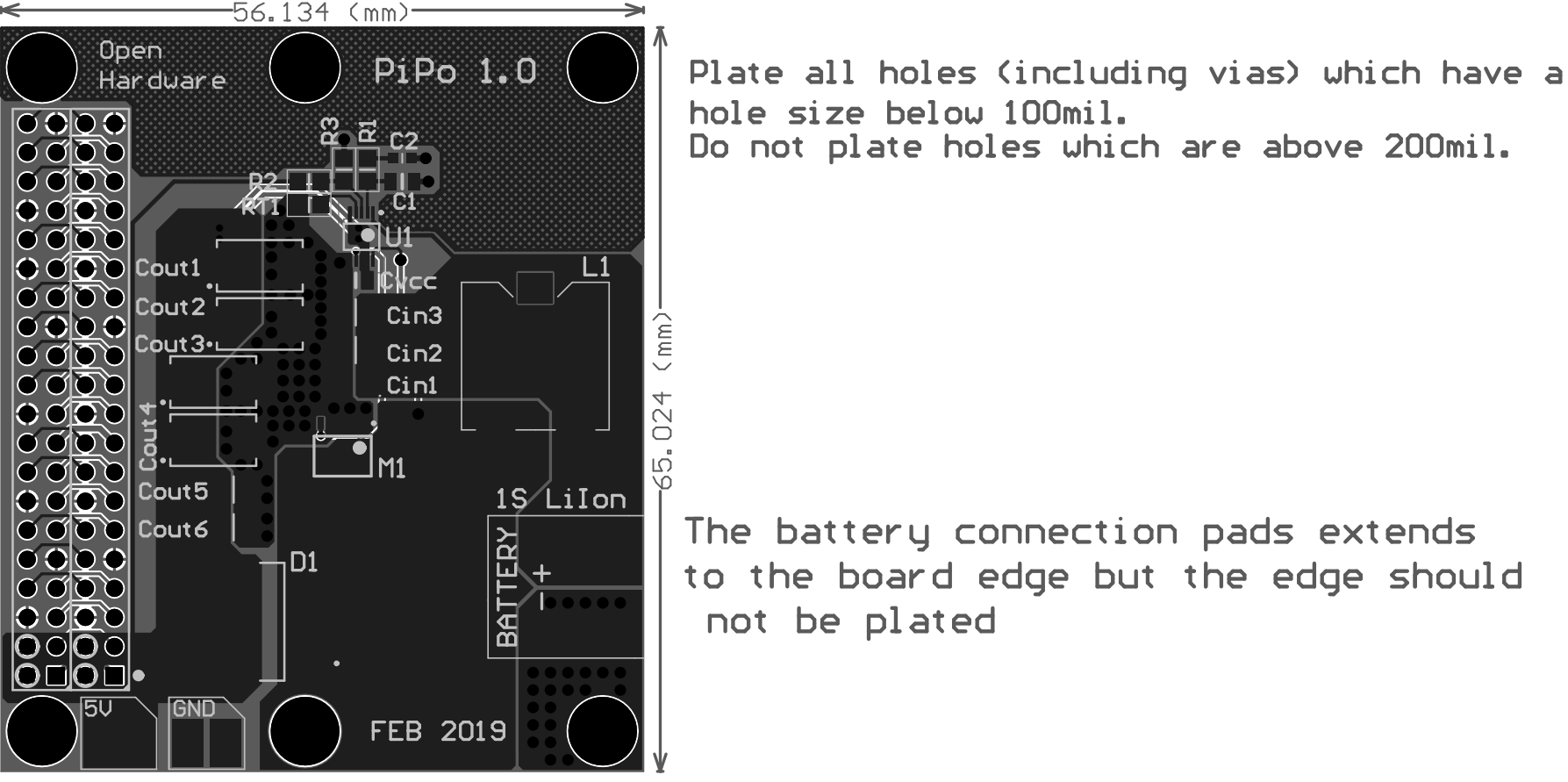
Composite:
Assembly:
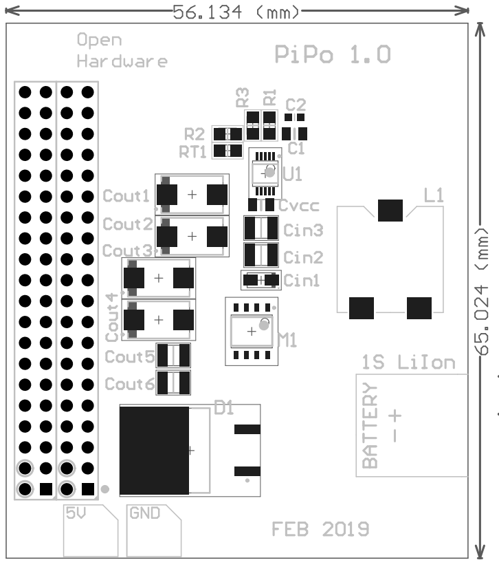
Comments on Revision 1.0 - Assistance regarding _PCB layout, component placing & the schematic design_ was taken from the corresponding datasheets. Output voltage was as expected, as well as the ability to supply high currents. However, on probing the output with and oscilloscope it was found that the output waveform was quite noisy and had significant switching noise at the frequency of the used DC-DC converter.
It was concluded that PCB layout and component placement were the culprits for induction of switching noise (To be addressed in rev 2.0). Hence, I would not recommend following the component placement and PCB layout guides present in LTC1871-1's datasheet. Instead, Understand the guidelines given and apply common mutual induction principles while designing the output section.
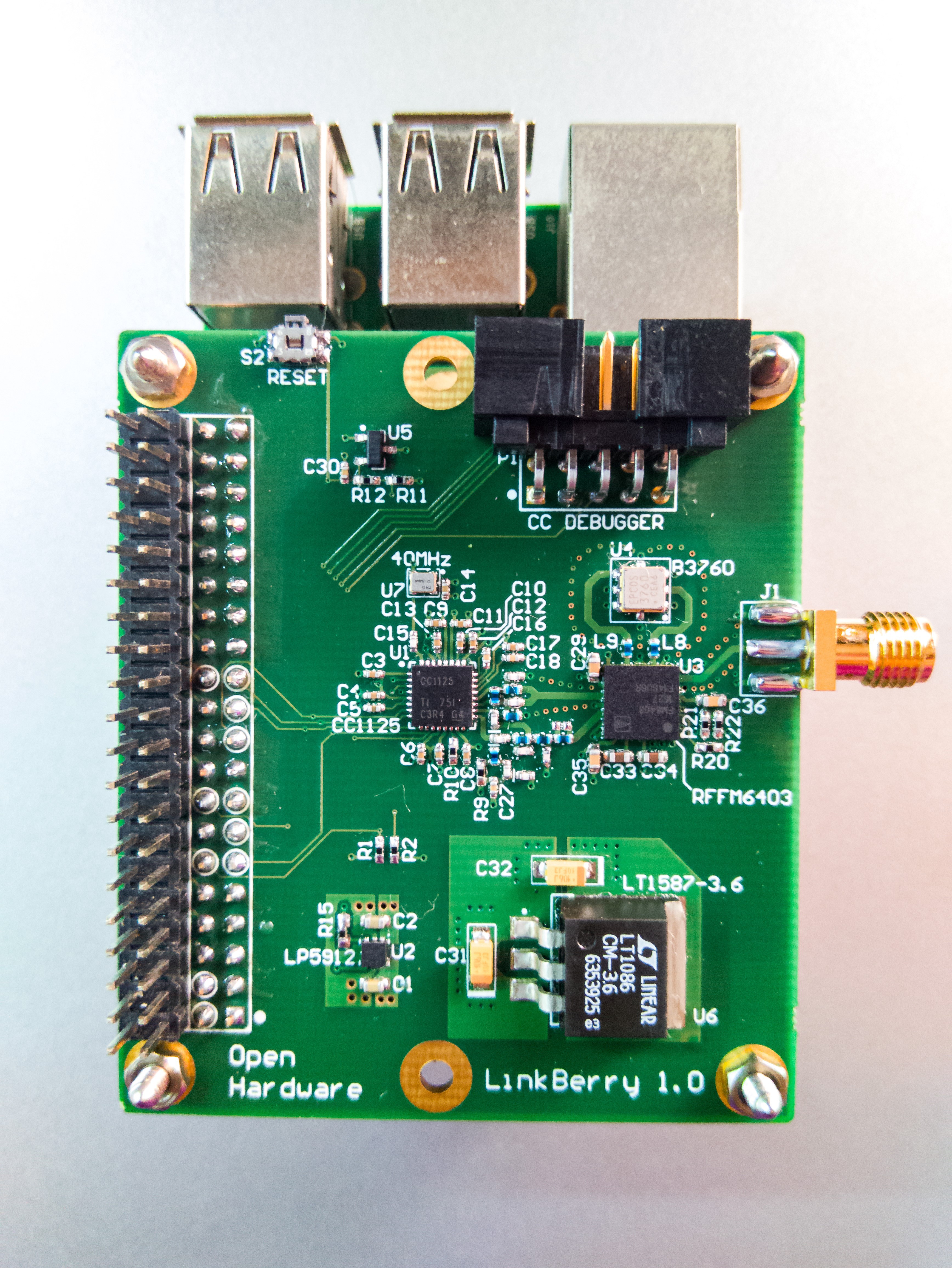
2. Transceiver Board (LinkBerry):
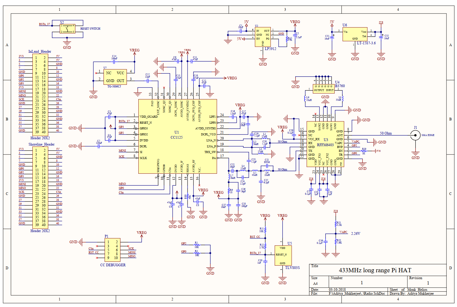
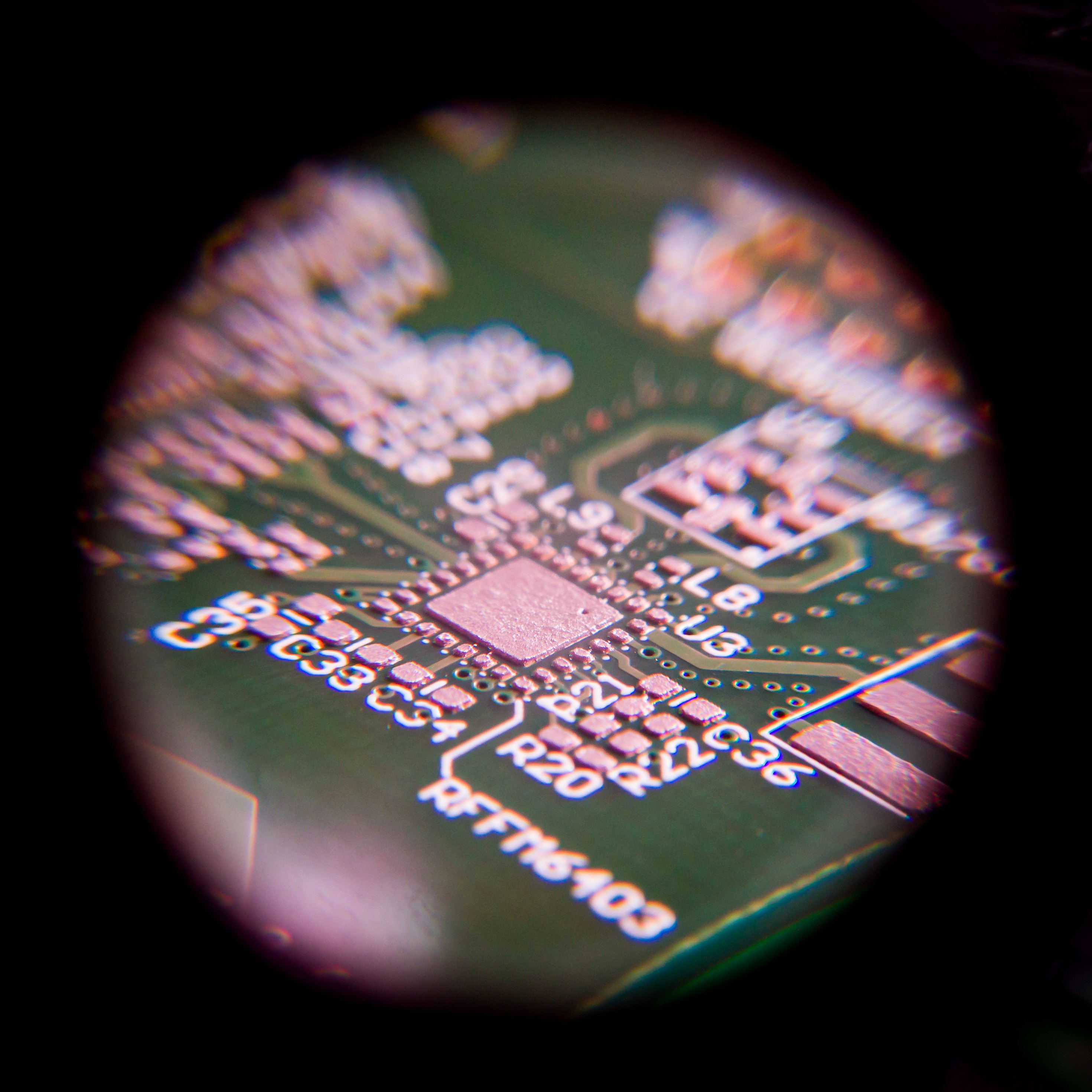
For telemetry, real time location update and live image/video feed a point to point long distance RF link was designed and fabricated which is based on Texas Instrument's CC1125 - a single chip, fully integrated narrow band RF transceiver. Coupled with a front end module (FEM) - Qorvo's RFFM6403, the board has a maximum output power level of 30dBm. The FEM has inbuilt selectable power amplifier (PA) for transmission and a low noise amplifier (LNA) for reception. This communication stack acts as a bridge between the Pi's SPI bus and the unguided RF encoded & modulated data. In other words this encodes, modulates & transmits data received over the SPI bus (from the Pi). Also it decodes data received over its RF link and sends it through the SPI bus.
This is a 4 layer board since this includes mixed signal components, hence, strict PCB layout requirements. Also a thinner dielectric (prepreg) between the 50 Ohm RF traces and the GND plane allows for narrower RF microstrip lines for a given impedance. So, the layer stackup is important to keep in mind while designing.
Schematic:
Schematic PDF
Layer stackup:
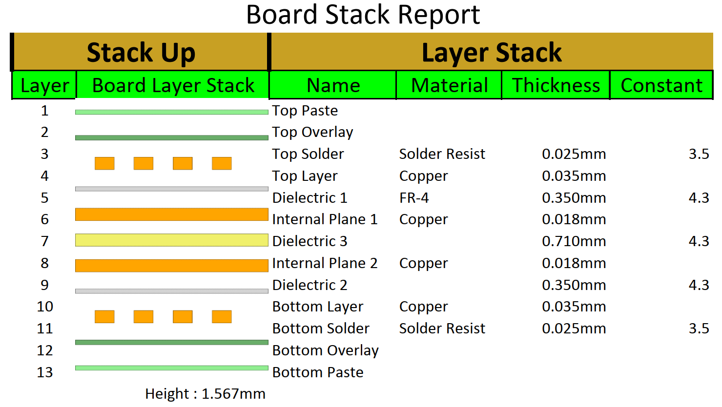
- Top layer - separated digital and analog signals, most important signals are routed on this layer.
- Internal plane 1 - GND plane.
- Internal plane 2 - Power plane includes 3.3V, 3.6V & 5V polygons.
- Bottom layer - less important digital signals, traces which did not fit on the top layer, bridges and a GND polygon.
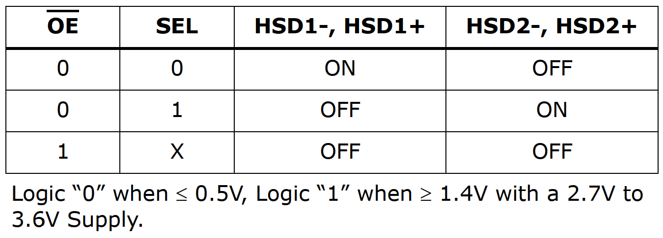
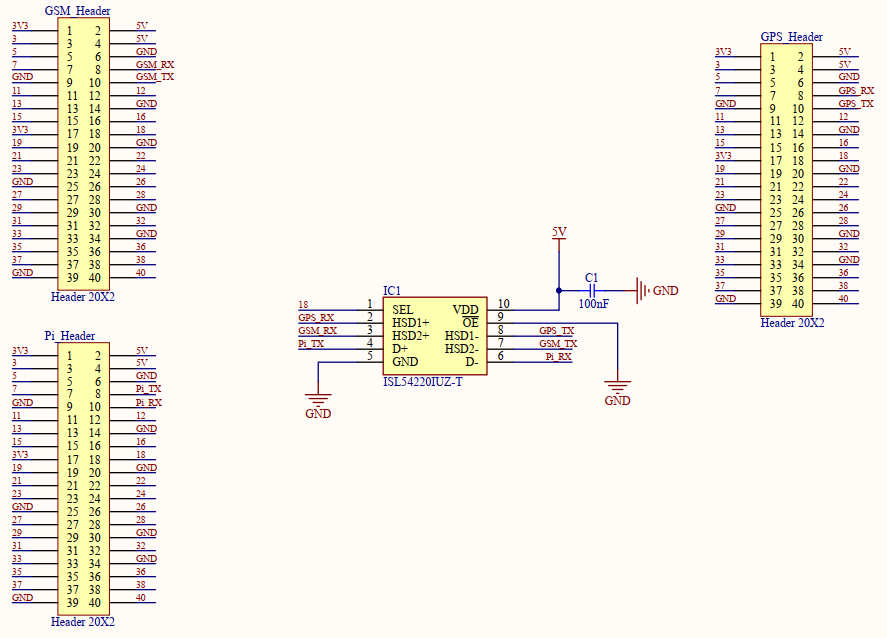
## 3. Multiplexer Board (PiMux):
This is a rather minimal 2:1 MUX board built around ISL54220 - a single supply dual 2:1 multiplexer that can operate from a single 2.7V to 5.5V supply. This multiplexes the two serial peripherals - GSM & GPS boards and enables them to be used one at a time on the single serial bus available on the Raspberry Pi. Data rates aren't a bottle neck as this IC was designed for USB purposes (480 Mbps).
Functional diagram:
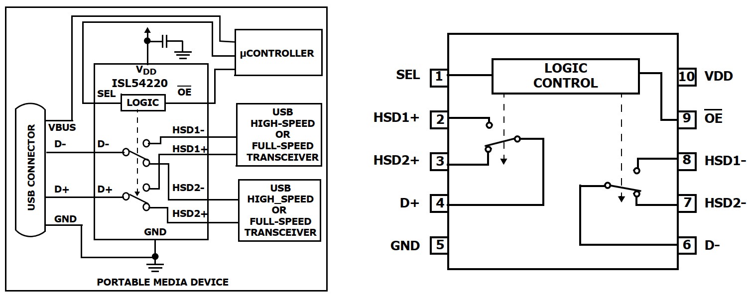
Truth table:
Schematic:
4. GSM board:
We used an available Raspberry Pi GSM hat made SmartElex. The primary purpose of GSM in this project would be to keep the communication link intact even if LOS communication is not possible. For example - maintaining comm link very near to ground where LOS might not be available. Also, for retrieval purposes the GPS and GSM board works hand in hand to provide the exact location where it landed. The GSM board is based on Quectel's M66 SMD module. So, relevant AT commands will be...
Read more »

 ensafatef
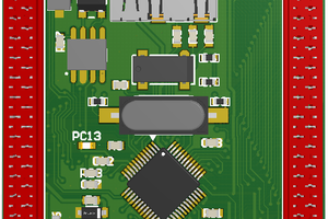
 Florian Eich
 jay-t
jay-t
 John Whittington
Nice design - have you flown it yet?