 Bharbour
Speaking with someone here on Hackaday, they mentioned that they were planning on using a Maxim MAX7219 chip for driving these displays. Out of curiosity, I decided to build a few boards to explore this chip. Perusing the data sheet, the MAX7221 looks like an updated version of the 7219.
Using these parts to drive a matrix LED is a little bit of an "off label" use. The data sheet talks about using these parts to drive up to 8 of the seven segment numeric displays, and not much about driving a matrix display. There is even a BCD to seven segment translator built in to the chips. On further reading, the translator can be bypassed, and the chip is designed to drive common cathode displays. The LTP2558 matrix displays that I have are common cathode displays.
These chips use SPI for communications instead of the I2C that the other two driver chips use.
With the I2C based chips, the target address specifies which chip on the bus that you are talking with. The ISSI chips that I used only support 4 different addresses, meaning that if you want more than 4 characters in the display, you have to break up the I2C bus. Address translators or bus mux chips are the two most obvious ways to do this. Either is expensive. Another method would be to use a controller with multiple I2C buses. This seems wasteful of resources, and adds cost, as you need to buy a higher pin count processor.
The SPI interface uses daisy chaining to build a bus up, and the physical order that you put the data on the bus determines which driver chip winds up with a particular word of data. As a result, there are no addressing limitations created by the SPI interface. There are some limits to how many devices can be put on a chain. There may be timing limitations since all the parts use the same chip select and clock signals to pass and store data. There are bus loading limitations, as it is necesary to drive the clock input and chip select input of every driver chip on the chain. Because of the higher data rates supported by SPI interfaces, expect to have to terminate the SPI bus to preserve signal integrity.
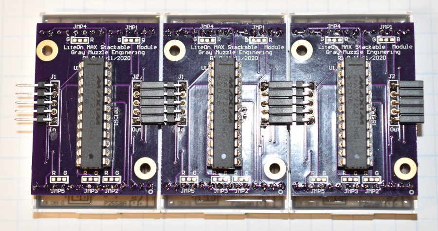
The biggest advantage that the MAX7219 or 7221 chips bring to the hobby world is that they are available in the old school DIP package, a 24 pin skinny DIP with 0.1" (2.54mm) lead pitch and 0.3" (7.62mm) spacing. These packages are very easy to solder without microscopes or other special tools and skills. They are also small enough to pack two of them on a board that sits on the back of the LTP2558 displays.
The biggest problem with these chips is that they are expensive. The 7219 chip lists at $8.91US and the 7221 chip lists at $9.26US in single quantities. The pricing does not fall very fast on the volume curve. Searching the net, some sites are offering the MAX7219 as cheaply as $1, but if it sounds too good to be true, it probably is.
Writing a driver for these chips is somewhat different than the I2C interfaced chips. With the I2C chips, you could write all of the On/Off control registers of one driver chip in a single I2C transaction. With the SPI interface, you can write one of the control registers of each chip on the chain in a single transaction, necessitating breaking up setting the LEDs into a transaction per display column. After some testing, you HAVE to write each chip in the chain every transaction or strange things happen and downstream characters get corrupted.
Both the I2C and the SPI device drivers use a character generator table to map the incoming ASCII character to the desired pattern of LEDs. The character generator table used for the MAX parts is identical to one of the ones used in the ISSI31FL3730 driver that I already have written. The MAX parts run 5 columns X 8 rows of LEDs in the matrix. The character generator table supports 96 different characters, one for each of the printable ASCII characters. A 2 dimensional array with 96 x 5 bytes holds the character generator table data. When the ASCII data array comes into the device driver function, it is translated into an array of pointers for the character generator table. Each incoming character becomes a pointer into the correct location in the character generator table for that character. A nested loop assembles a column register address and the correct column data for each character into a transmit buffer. At the end of the inner loop, the transmit buffer is sent out to all of the driver chips in the chain. The outer loop iterates until all 5 of the columns for the characters have been sent. This is considerably more complex than the I2C driver.
One "feature" of the SPI chain is that the first byte out of the bus controller winds up in the last driver chip in the chain. This means that the physical SPI chain should run from right to left through the driver chips so that the first character data winds up in the leftmost driver chip. Obviously, it is possible to reverse the order in software, but the driver is already complex enough.
On the previous driver boards that I designed, there is a single connector for the power input and the I2C bus. This required making a messy cable with a tap for each character. For the new boards, I pass the data through the boards with an input connector and an output connector. The boards will stack side by side for the length of the chain with no cable between the displays. This method reduces the flexability on picking the character to character spacing though.
Each LTP2558 display has a separate red and a green 5x8 matrix. I designed two boards using a single MAX7332 chip with jumper selection for the color. Personally, I like the green better, so I made a default connection to the green matrix. If it were necesary to run the red matrix, the jumpers can be cut and the red selection made with a soldered in jumper. I don't think it will be possible to run both the red and green matrices at the same time, from the same driver chip. The forward voltage of the red and green LEDs is different enough that the green LEDs would probably not be visible at the operating voltage of the red LEDs. This has not been tested though.


After having the first version of boards to determine the inter-board stacking distance, I did another version that stacks the boards in contact with each other. This will require a new driver methodology to drive. The character generator arrays used on the other displays take advantage of the ability to space the characters with the display module mounting. The driver system is completely character oriented. One characters data goes to one LED module. The non-spaced modules are a continuous array of LEDs. To take advantage of the non-spaced LED display system, the driver is probably going to look more like a video frame buffer.

The internal organization of data in the MAX7221 chips is by LED column, so the "continuous" scan path becomes the vertical column. Video Systems generally have the scan path horizontal. If you look carefully at the edges of the display modules, you can see mechanical keying notches to help align the modules when they are in contact with each other.
Both of the board designs shown above only support a single color, defaulting to green.
A final iteration of this driver board will probably have extra connector sites so that the same PCB can be built as either a non-spaced board or with mechanical spacing between the LED modules.
In order to support the three possible colors, I laid out another driver board with two MAX7221 parts, one for red and one for green. The option to drive either or both red and green, 2 of the MAX7221 chips are needed. This gets expensive quickly. I did not use the plug pass through method on these boards because the power supply current can get pretty large with the possibility of running both matrices at the same time. In testing, I have seen 400mA per display in some situations and the pass through connectors are only rated at 3A per pin. Also, the power ground and the SPI ground share a common pin.

The SPI cable interconnect arrangement is showing some signal integrity problems and requires a terminator at the end of the cable to get reliable communications. Neither of the PCB daisy chain designs required termination to operate reliably, though that may change as the number of modules on the chain increases.
Discussions
Become a Hackaday.io Member
Create an account to leave a comment. Already have an account? Log In.