 Paul McClay
update: at end add note re offset
(this entry mostly copied from #Minamil: a minimal CNC mill - HaDP 2021 -- the Hackaday Prize flavor of this project -- where it started while I'm working out how to deal with the two projects)
Lots of chips have power & ground in the same two corners. How about bypassing on the breakout where it can do some good?
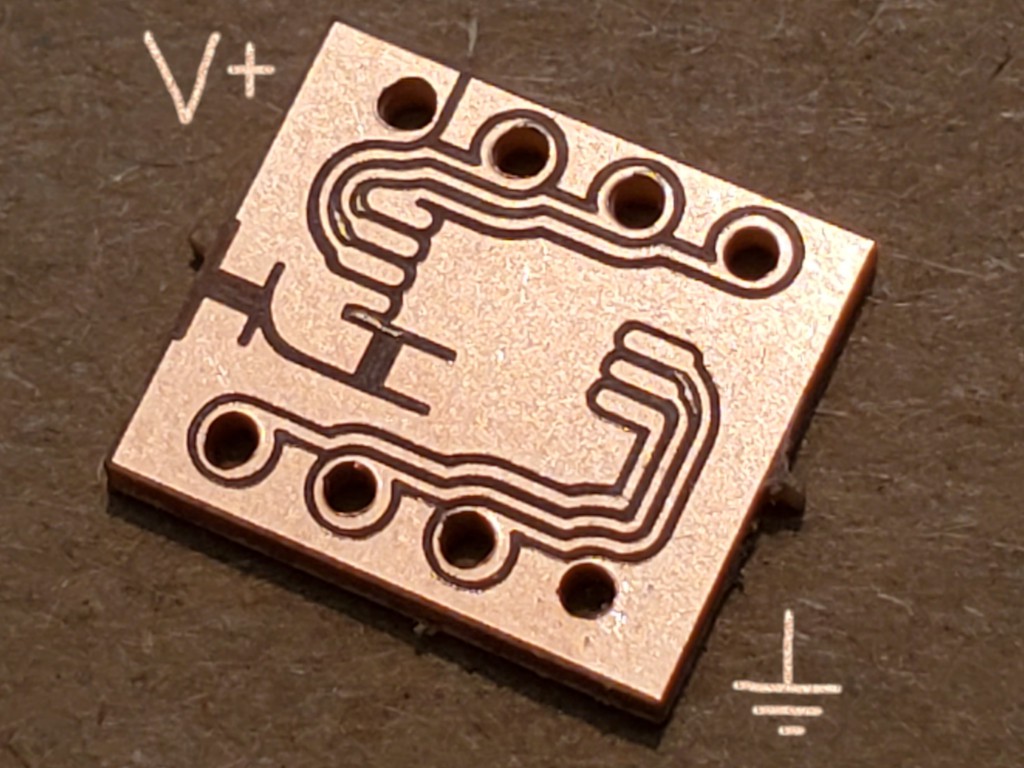
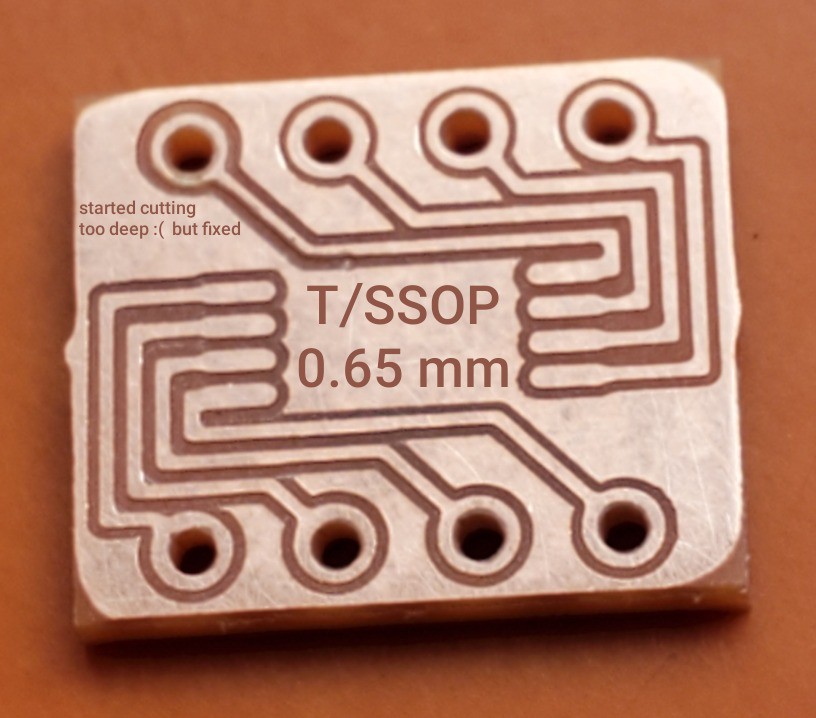
Earlier I milled a simple T/SSOP-8 breakout board to validate milling for 0.65mm pin pitch.
While doing that I checked what I might have in SSOP-8 to put on it and found some MAX4326 op amps on an old laptop mobo. The datasheet recommends two bypass capacitors ",,,as close as possible to the device supply voltage input [and] the ground end of these capacitors near the ground plane...", which is likely serviceable for nearly any 8-pin dual op amp, and also for many other 8-pin packages. [note 1]
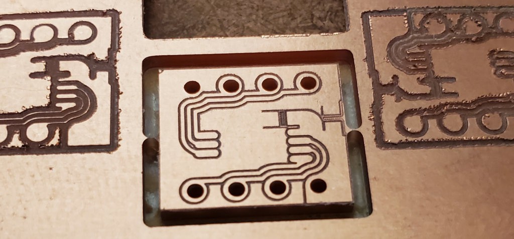
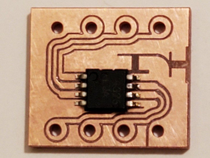
Hmm. Only single-side copper-clad board on hand, so no ground plane. Can I do something with a single copper plane? Doodle doodle... maybe so. First try shown above.
Yes, there's a loop in the ground trace -- it's really small. I haven't tried to figure at what frequency it would start to matter but I'm pretty sure it's a disregardably large number of 10ᵐᵃⁿʸ Hz for anything in DIP-8.
Actually this project is supposed to be more about milling than PCB design so... The adjacent traces are 16mil (0.4mm) center-center. The traces and grooves look pretty close to the same width, or about 8mil (0.2mm) each. Each groove cut in two passes about 3mil (0.07mm) apart. That suggests it's cutting about a 5mil (0.13mm) groove. The paths around these little islands where the two outlines diverge a little are not far from 5/8 the width of the rest of the grooves, so that seems to be about right.
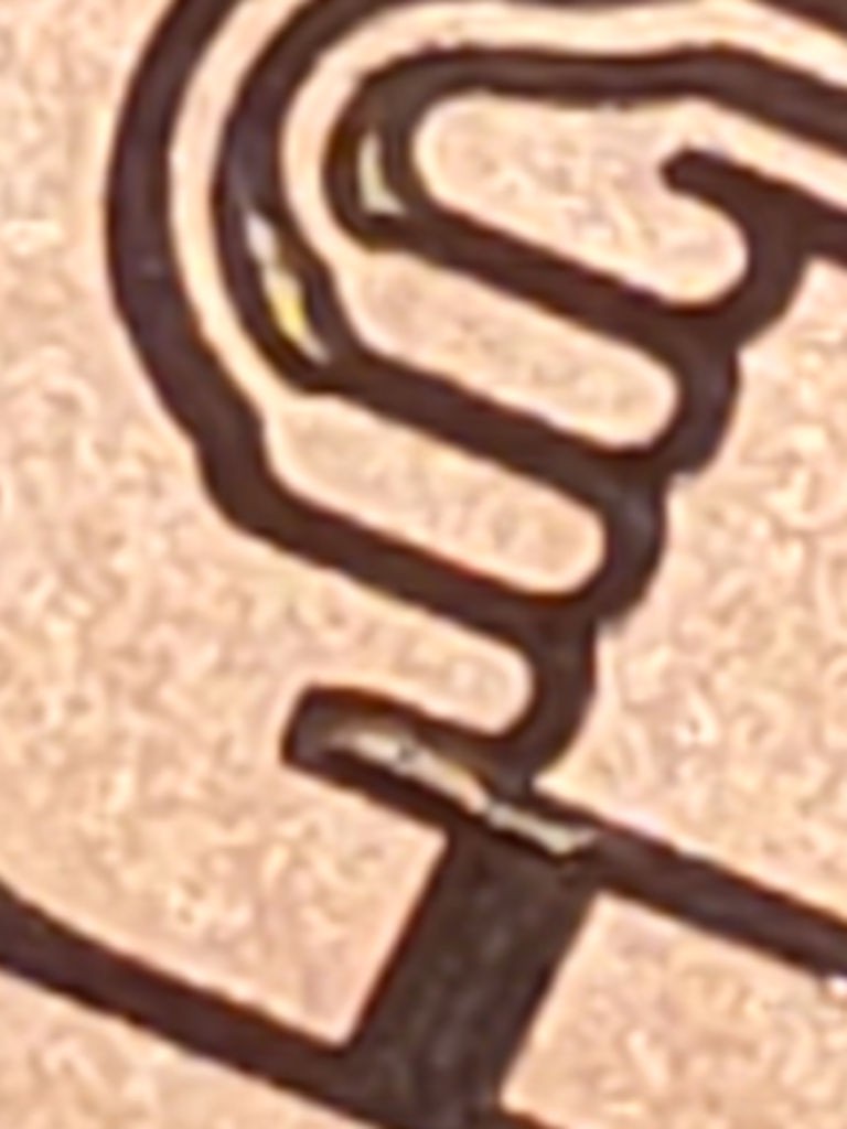
Cut with a 0.1mm 20° V-bit. That's pretty small runout - which is mostly about the nice spindle - which doesn't really fit the "cheap"/accessibility theme unless you already have one. However the generality of the separate rotary tool allows amortizing its cost, whatever that may be, over many other uses. The point being that the little mill can make good use of a good spindle. Given a nominal tool diameter smaller than the trace separation, FlatCAM generated toolpaths with a little separation between the adjacent trace outlines, which made room for an additional small loop to fully clear the space between the capacitor lands. The space between the capacitor and the chip supply pin was too wide to clear with two outlines but not wide enough to fit another full loop (fit four outlines) so a little island remains.
LESSON: designing a PCB for isolation milling with simple offset outlines requires more attention to tool path widths - and overlaps. Kinda like designing features as multiples of shell thickness in 3d-printing, but for even multiples of tool size if using simple outlines. Or smarter software that can pick up uncut slivers between offset outlines... which is not trivial... for small pass overlaps.
SO MAYBE: Geometrically, I think limiting "pass overlap" (stepover) to a tick over (under) 50% might solve a lot of that. (Or a more clever approach like #PCB Isolation Routing Software.)
To be clear, this isn't all about stuffing a fancy $pindle in the cheapest mill. An old garage-sale Dremel® cut lines of two passes that look like less than half of 20mil (0.5mm) center-center in the prior example:
...so it should be able to cut traces on 16mil centers too. That earlier example was set up for a bit diameter closer to the designed clearance between traces, so the two outlines in each groove were practically on top of each other with very little separation, which gives 3mil back to the Dremel.
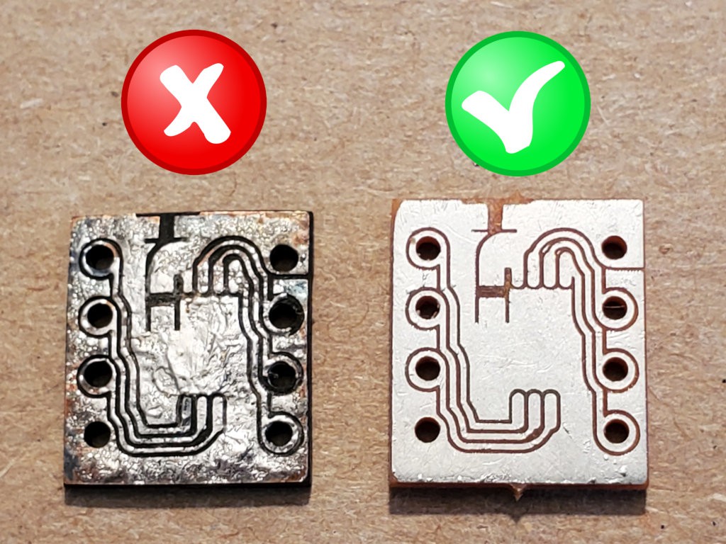
Cutting this bypassed breakout took more tries (time) than really needed if I had a better idea of how to use the tool.
This picture shows the first (left) and last (right) attempts to cut the little breakout:
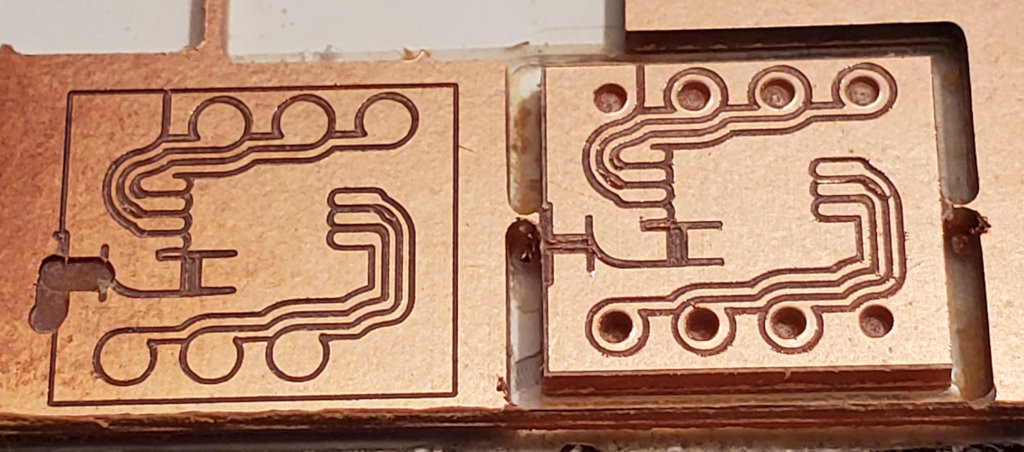
On the first try (left) I got a clean outline, then forgot to load new gcode after changing bits to bore the through-holes. In hindsight, I think that looks like I could have finished it and been done - because the bigger bit only went between a pair of capacitor lands and I think a cap would still bridge that gap. After promptly interrupting the wrong gcode, I could have recognized that the goof wasn't mortal and simply loaded the correct gcode and finished the board. But I didn't.
The last one (right) came out pretty well, except that the through-holes don't go through. They were bored from near left, left-to-right, then the far row left-to-right -- and get shallower in that order. That answered whether or not I could get away with drilling them with the end mill I was using (answer: not for long). Something got failure started, then it got duller in each hole. After that it just polished the copper outline for a few passes before breaking through the copper plate and cutting incompletely through the board, slipping Z steps. It finished the outline ok after I changed the cutter & re-set Z. If I were better at thinking about what I'm doing with this tool, I would have chucked up a 1mm drill and run the drilling code again to finish the part. But I didn't.
The holes off center in the copper pads show one of two imperfections (I don't remember which for which piece): 1) homing is kinda soppy with my current limit switch arrangement - and I screw up often enough to loose position often enough for that to matter, or 2) something moves while changing bits, and I don't know what yet.
Question: can 1mm (or 0.9mm for less over-sized through-holes) "corn cob" milling cutters drill too?
And there were other attempts between first and last:
The middle one is ok, but the operations are imperfectly aligned because I screwed up something and lost position (and homing remains imperfect). The flanking attempts got cut too deep while I was confused by a peculiarity of Z probing & autoleveling in bCNC: the position after a Z-probe is where Z stopped not where the probe triggered (unless, perhaps, if moving v...e...r...y slowly) while autoleveling uses the probed values.
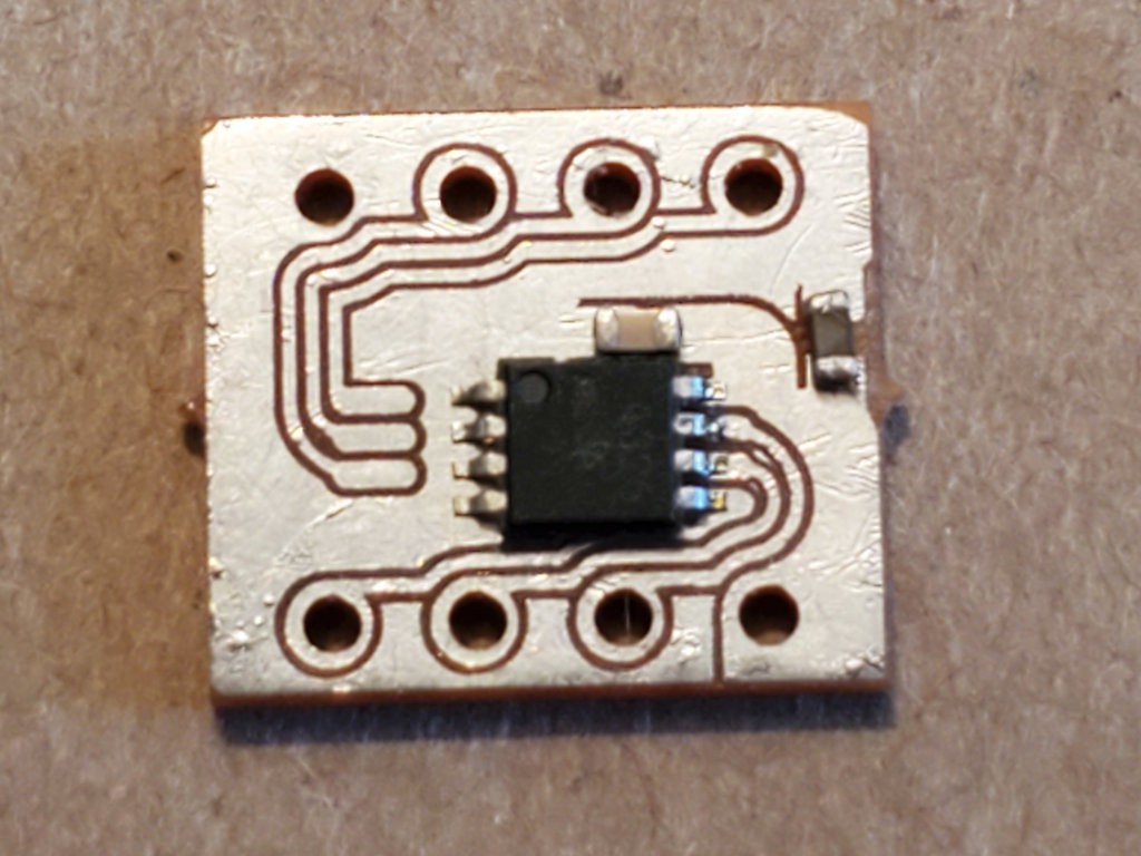
Then I tried a couple of ways to tin a PCB, one of which worked:
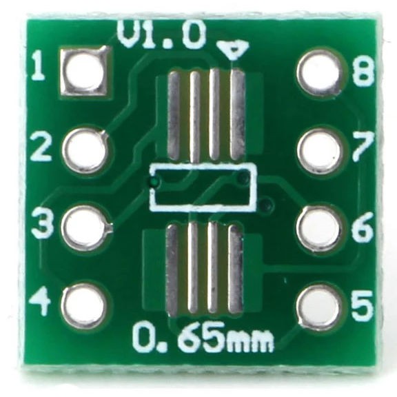
And then I remembered that SSOP packages can have different widths:
I knew that; just wasn't thinking of it while drawing traces. That would be why commercial T/SSOP8 breakouts have super long lands:
FITNR, maybe.
teaser... {time passes} ...click for delivery:
̶D̶u̶n̶n̶o̶ ̶w̶h̶y̶ drill holes are offset... {time passes} ...because the Proxxon strapped into Dremel-shaped clamp saddles wasn't really vertical so different length bits touched down at slightly different positions.
Note
[1] 0.1µF and ≥1µF. Overkill apart from narrow edge cases, I suspect, especially with same size/package (i.e. inductance) caps. I had a more compelling story in mind for using both caps but was thinking of a different amp + not thinking of other stuff. One 1µF MLCC + fatter trace area might work better. But I'm just making stuff up unimpeded by actual competence. It's so much easier that way.
Discussions
Become a Hackaday.io Member
Create an account to leave a comment. Already have an account? Log In.