Nick Sayer
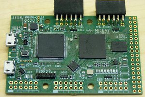
This project isn't perfectly defined yet, but at the outset, the goal is to support as many of the different AVR programming modes as possible. That means ISP, PDI, TPI and UPDI. Of those, PDI, TPI and UPDI are quite similar (a bidirectional async serial pin and for PDI, a clock), and ISP is the oddball. However, it turns out that the XMega64D4 has MOSI, MISO and SCK superimposed on the same pins as TXD0, RXD0 and XCLK. The only extra requirement is the ability to impose the TXD/MOSI pin onto the RXD/MISO pin when using those modes. This can be done with a GPIO pin to switch a buffer on (exact circuit TBD).
With my other programmers, I've used switches to change the programming voltage, but here I think I'd rather have the availability of 5 volts, 3.3 volts or target power available programmatically (of course, the controller itself would have to run at 3.3 volts).
Port C and D both have a USART and SPI interfaces. Since we need 2 SPI interfaces (one for programming, one for the SD card), I had to upgrade to it from the XMega E series. Port C will go to the SD card slot. In addition to the normal 4 SPI signals for the SD card, there will also be a power switch. This will facilitate a "card reload" operation that will re-mount the card and re-probe the filesystem.
Port A will be connected to the LCD - it'll be run in 4 bit mode, so 4 pins for D4-D7, and one pin each for E, R/!W and RS. The LCD itself is designed to run on 5 volts, but it can run on 3.3 volts just fine (the backlight would be dimmer, but we can give the backlight 5 volts independently). The trick is that the Vo pin must be about 4.5 volts lower than Vcc. If Vcc is 3.3, then that means Vo must be negative. That's ok, though. Normally a "contrast" trimpot is used to set this voltage somewhere between Vcc and ground, but if you use a charge pump to invert the 3.3 volt supply then you can anchor the ends of the trimpot on -3.3v and ground instead. Adding a charge pump is a slight annoyance, but it's only one SOT23-6 chip and two caps.
Port B will be for the 4 buttons.
Port D is where most of the programming controls are. The SPI port is 3 of the pins, plus the !SS pin is used as the target !RESET signal. For the synchronous serial modes, the USART's alternate pinning option is selected instead, which winds up being transparent at the hardware level.
To control other aspects, a number of GPIO lines are required - these come from the remaining pins on port D and E. Two of them enable 5 volt or 3.3 volt target power. Alternatively, you can leave both off to force target power. Another line is the TX/RX combiner line. This is required for TPI, PDI and UPDI. It enables a buffer chip to send a copy of the TX line to merge with the RX line, through a protection resistor. This happens on the target side of the buffering system. Another pin is used to change the !RESET target pin from a straight low to a copy of the clock. This is necessary for PDI programming. Another pair of pins are used for HV programming control for TPI and UPDI. In the case of TPI, this asserts 12 volts on top of !RESET to force TPI mode when the !RESET pin is disabled. For UPDI, this asserts 12 volts as a pulse on the UPDI data pin to force UPDI mode similarly when that pin is fused for GPIO use. These HV voltages are enabled with a P MOSFET and Schottky diodes are used to protect the !RESET buffer chip, and a resistor and zener are used to protect the MISO/DATA buffer chip. The HV voltage itself comes from a boost converter that is itself powered by the 5 volt rail.
System power will come via a USB C jack. The data pins are not (currently) used, and PD negotiation is not required, as the whole system will run on 5 volts at less than 5 watts.
The SD card is going to have a FAT filesystem on it. The top directory has a directory for each project. The system will make the top level menu from the names of these directories.
Inside each project directory is a CHIP.TXT file. This...
Read more »
 jaromir.sukuba
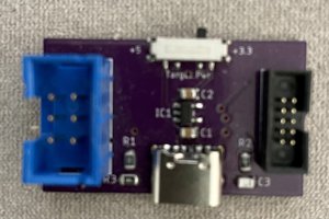
 Viktor Nikolov