Close
0%
0%

Photon

Open source UV curing wand

Similar projects worth following
This project is the answer to "Field Ready '' team to develop an open source, cost effective, and energy efficient UV curing tool that can easily be fabricated in remote areas.

Applications for such devices are wide, and include: PCB Solder mask curing, PCB conformal coating curing, curing of epoxy resin or acrylic UV sensitive adhesives, curing of UV sensitive encapsulating compounds, curing of 3D printed polymers and many more.

With advances in development of UV sensitive polymers, adhesives and resins, UV curing devices have become an important part of many industries.

Commercially available UV curing systems can be divided into:

UV FLOOD CURE SYSTEMS - LOCTITE UVALOC 1000

Flood systems are used when illumination of large surface area and/or large thickness of UV sensitive compounds are needed. Due to the high power of undirected light needed, mercury-vapor lamps are used.

STATIONARY UV SPOT CURE SYSTEMS - LOCTITE 97034

Spot systems are used when illumination of a small contact surface is needed. This is the most common industrial application. Systems like this use mercury-vapor lamps that are directed with a light guide to a pen shaped tool that is practical for operator use.

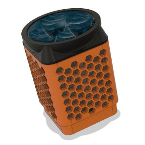
PORTABLE UV SPOT CURE SYSTEMS - EQ CL32

Unlike the previous group they use LED diodes which makes them portable. Improvement in spectral characteristics of UV sensitive compounds and LED technology has made portable UV wands sufficient for most spot curing applications. LED spot curing wands like Loctite EQ CL32 look like pretty nice and useful tools, but due to the high price of >1000$ they remain out of reach for common hobbyists, small businesses and organizations like Field Ready. Goal of this project is to make a cost effective alternative.

To design a successful product it is necessary to lay out design requirements and specifications.

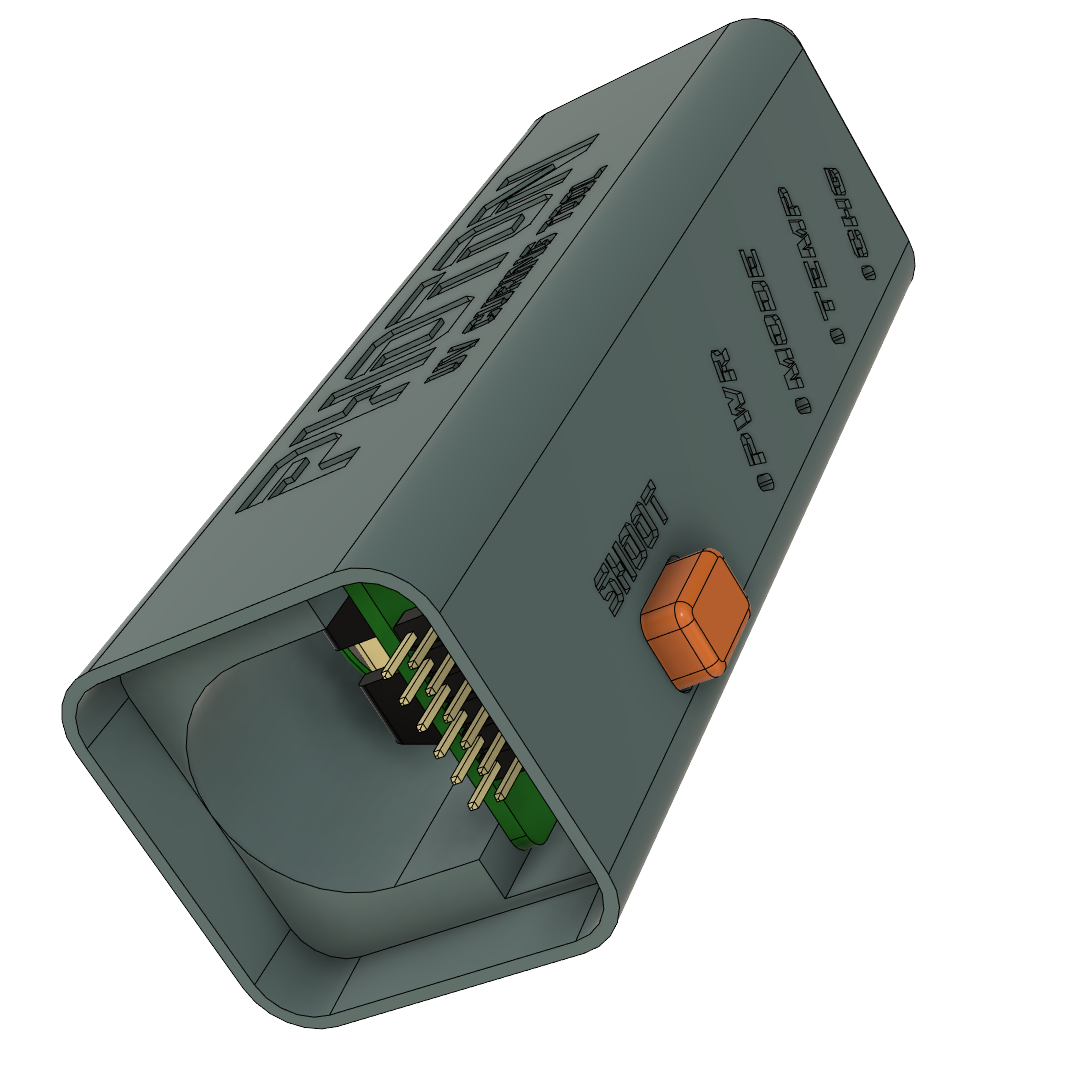
  1. Low cost of manufacture.
  2. Ease of manufacture & assembly.
  3. Energy efficiency.
  4. Support for multiple wavelengths in the UV-A spectrum.
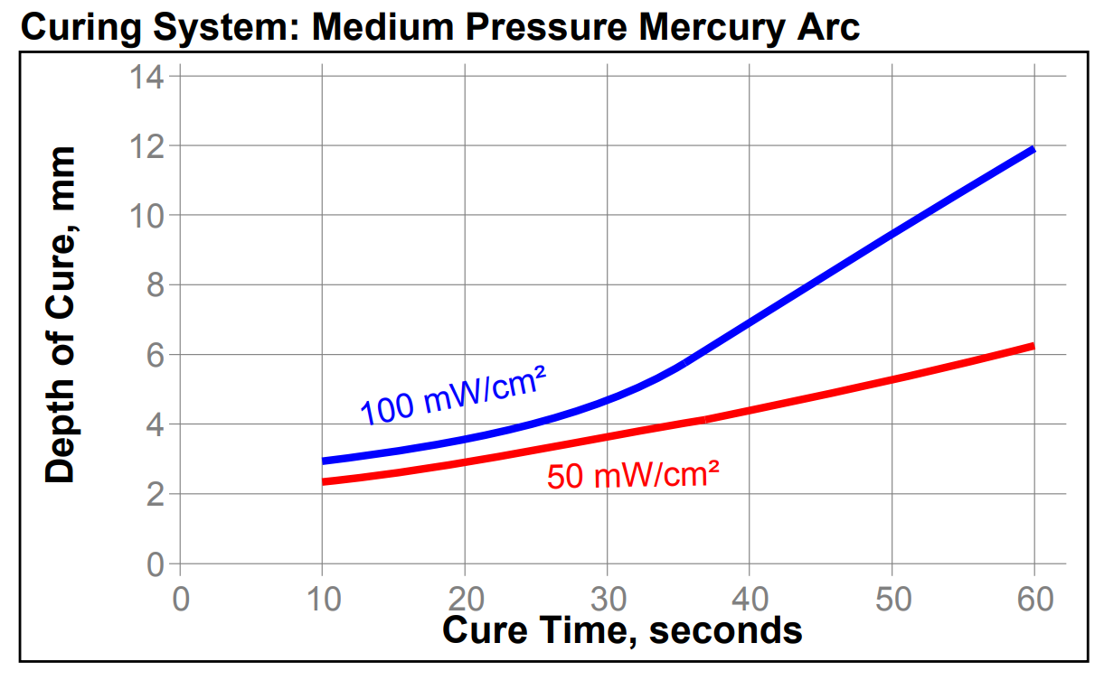
  5. Irradiated power of 100 mW/cm² or more.

LOW COST OF MANUFACTURE

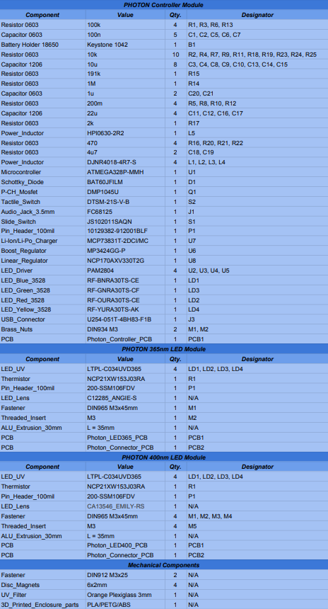
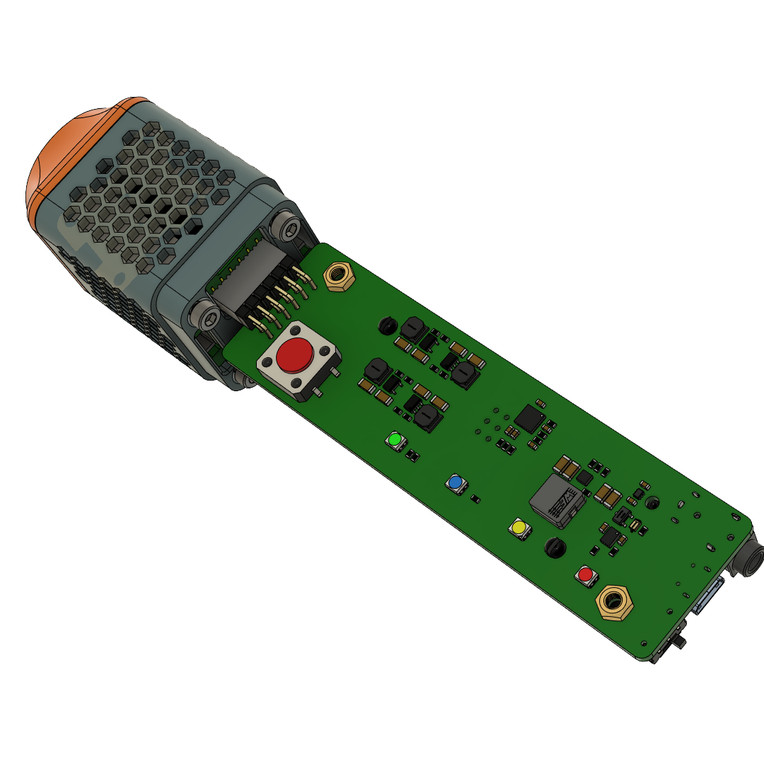
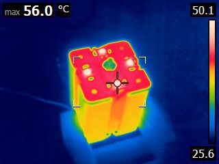
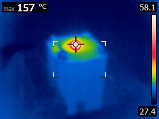
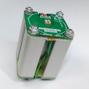
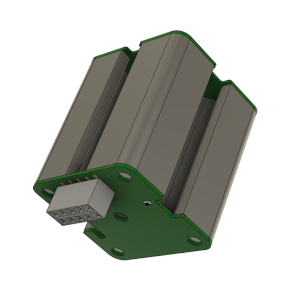
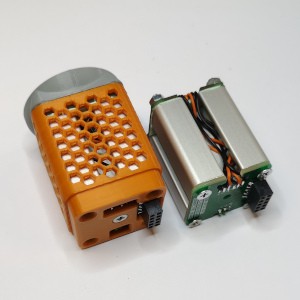
Big companies like Henkel(Loctite) have big logistical expenses while designing their products. Since I am working on my own and in my free time I don't. Low cost of device manufacture will be achieved with use of generic, industry standard electronic components and 3D printing of enclosure. One example of keeping the costs down is use of generic extruded aluminium profiles instead of a specialized heatsink to cool down the LEDs. Documented in this project log.

EASE OF MANUFACTURE & ASSEMBLY

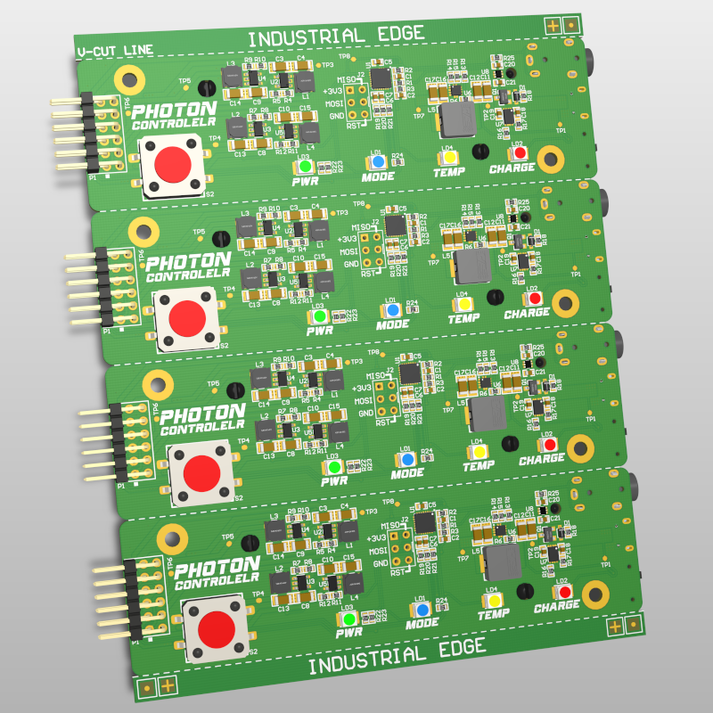
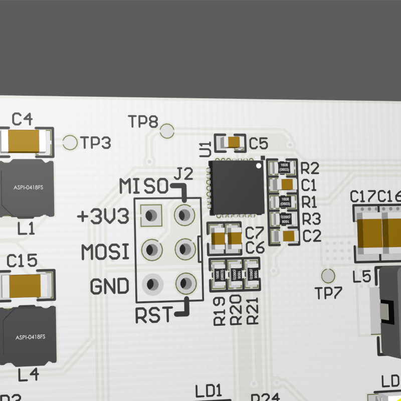
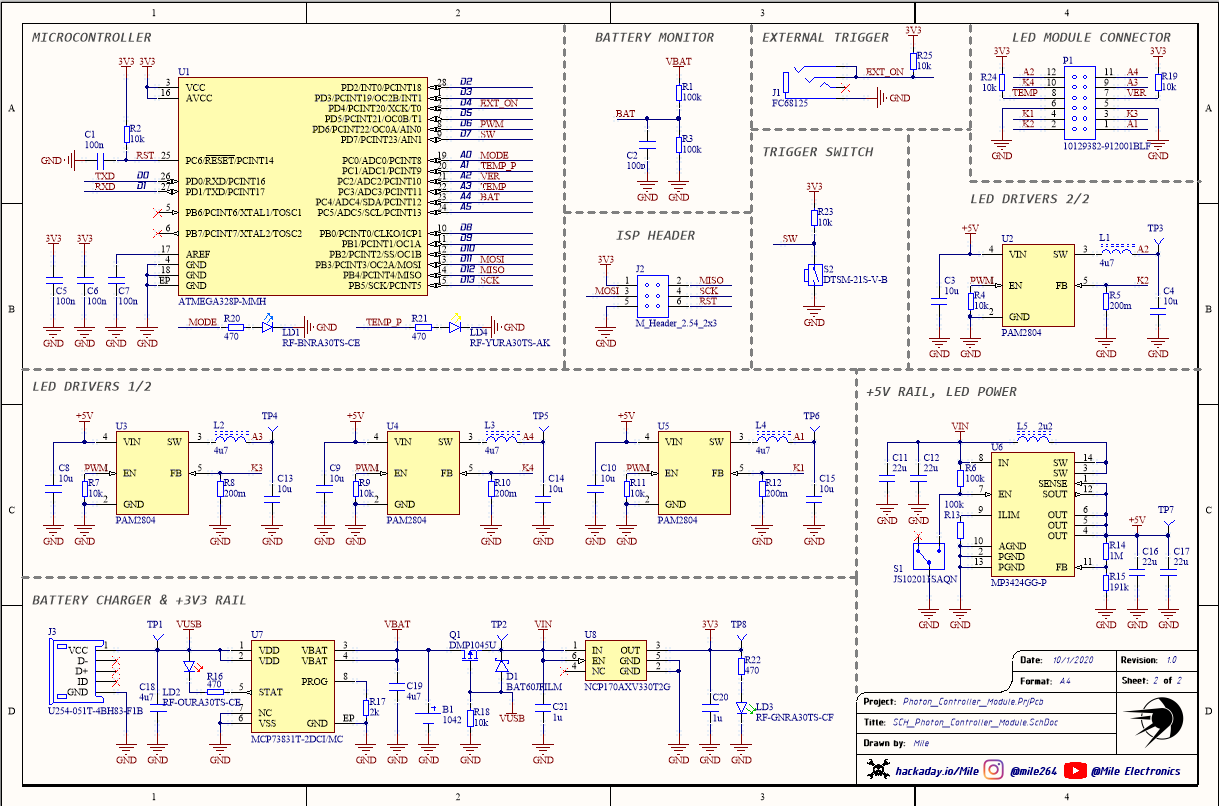
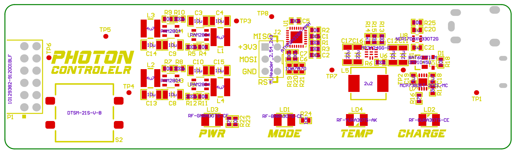
Special care will be taken to make PCB design suitable for hand and machine assembly to keep it accessible and make it scalable for bigger production runs. Detailed documentation will make the assembly process as efficient as possible.

ENERGY EFFICIENCY

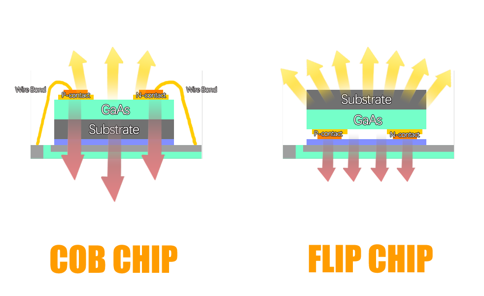
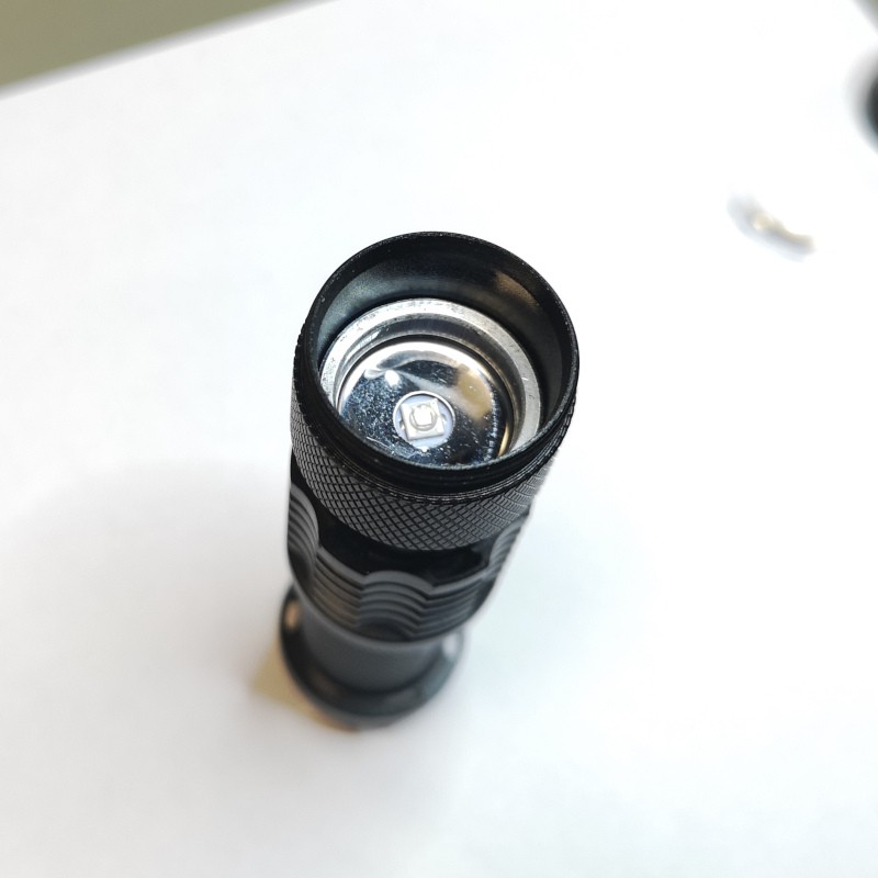
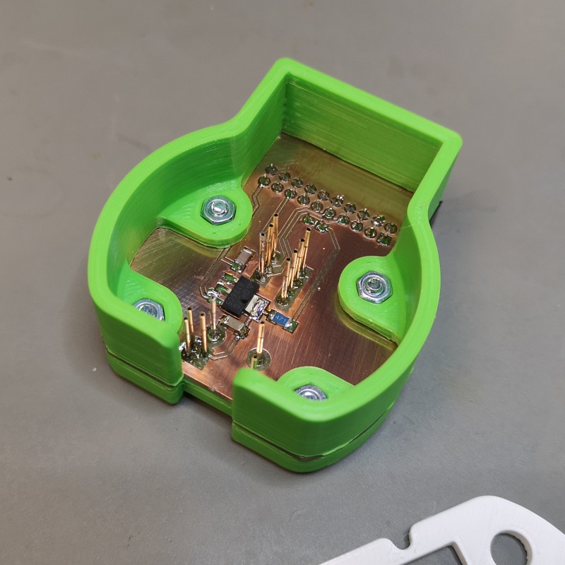
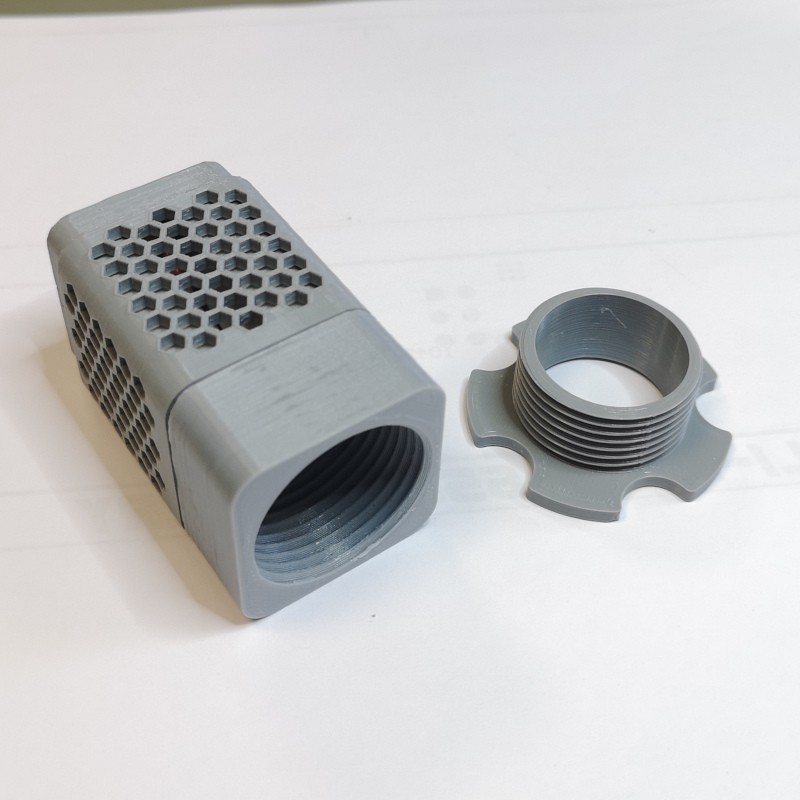
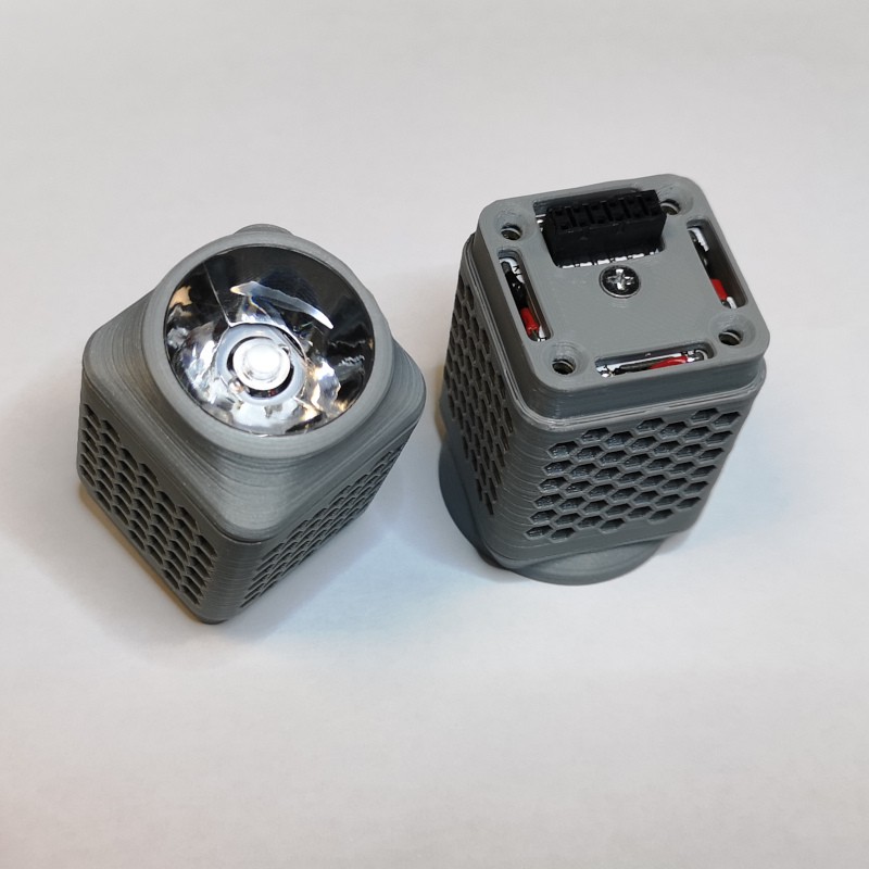
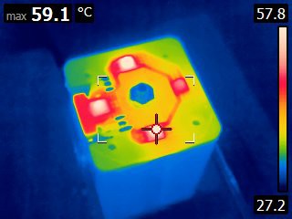
Efficient device means better autonomy when operating from an internal built in battery. Maximum efficiency will be achieved with use of the newest switching LED drivers, LED emitters and carefully dimensioned thermals. One example of the newest technology on the market is CSP LED. Opposed to traditional wire bonded die LEDs this type of LED offers better thermal characteristics and more irradiated power per surface area.

SUPPORT FOR MULTIPLE WAVELENGTHS IN THE UV-A SPECTRUM.

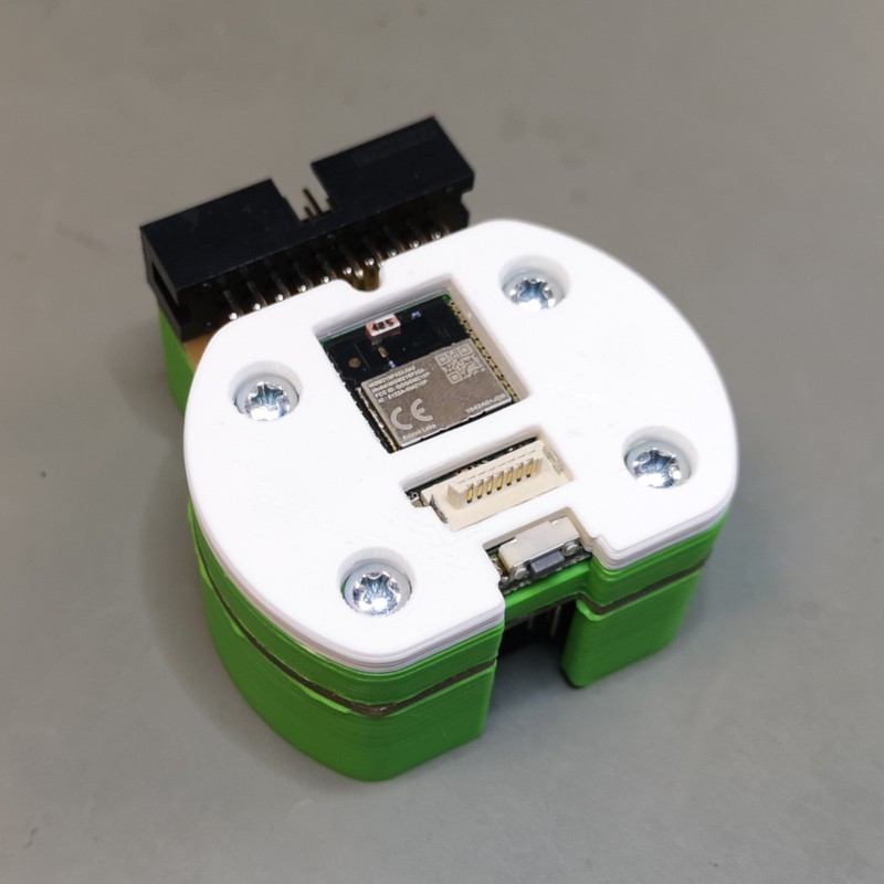
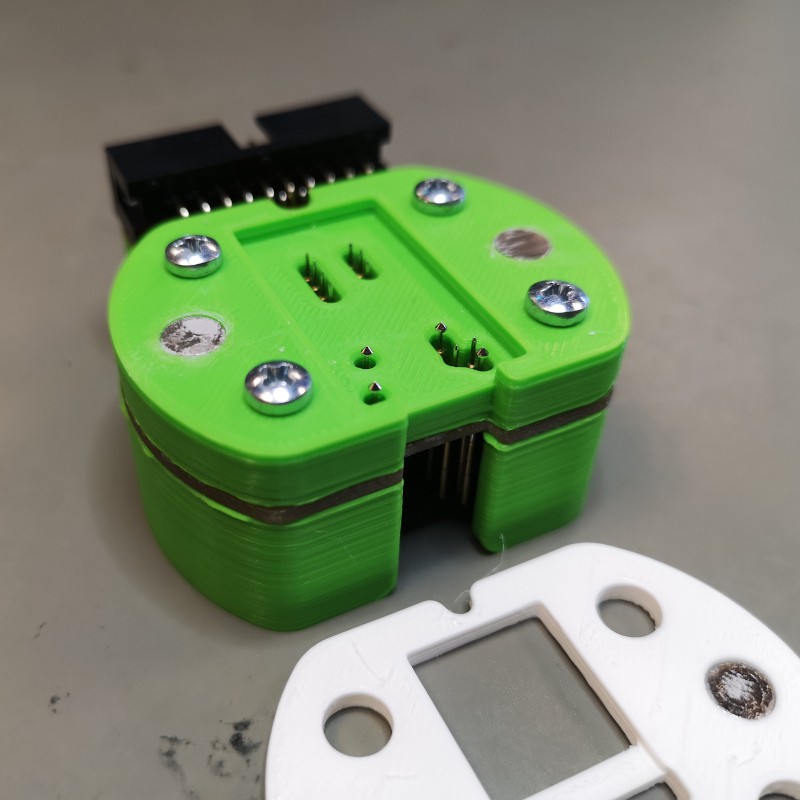
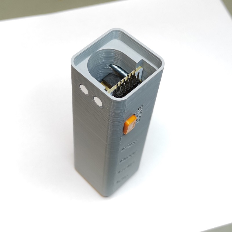
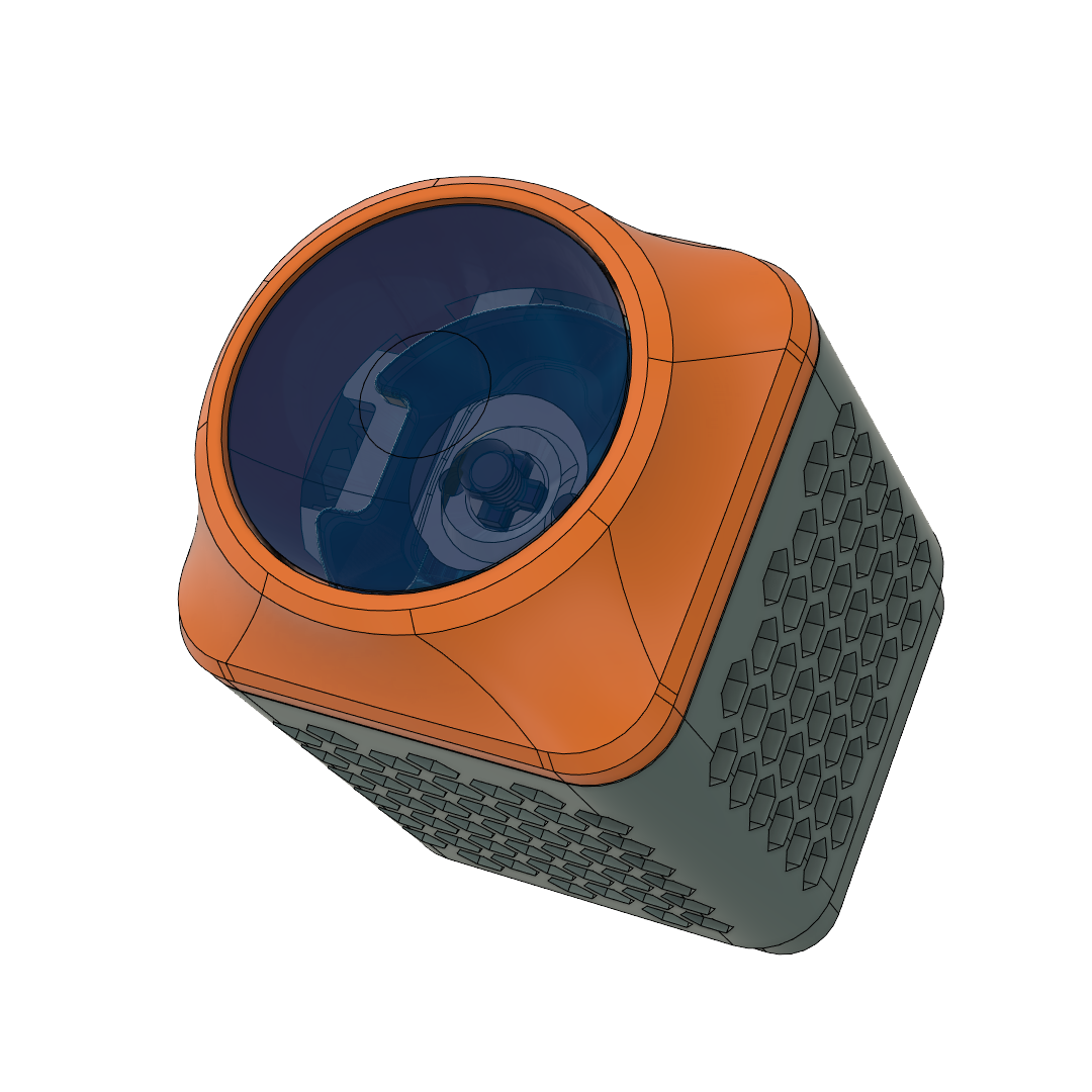
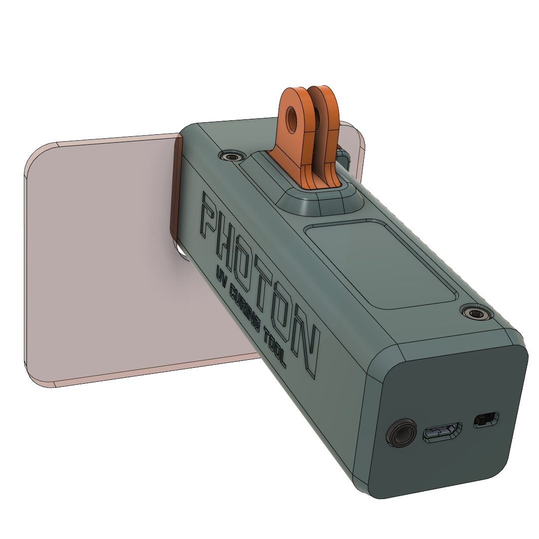
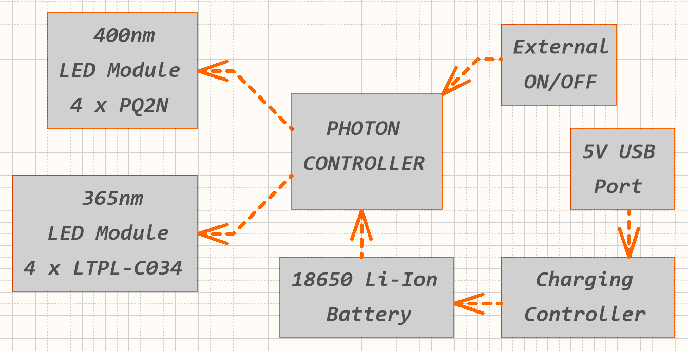
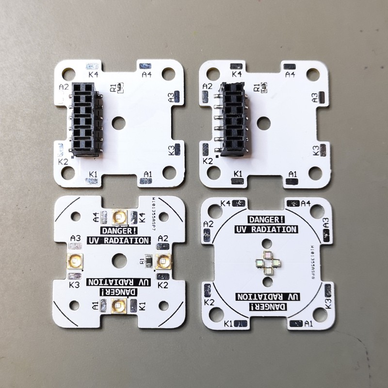
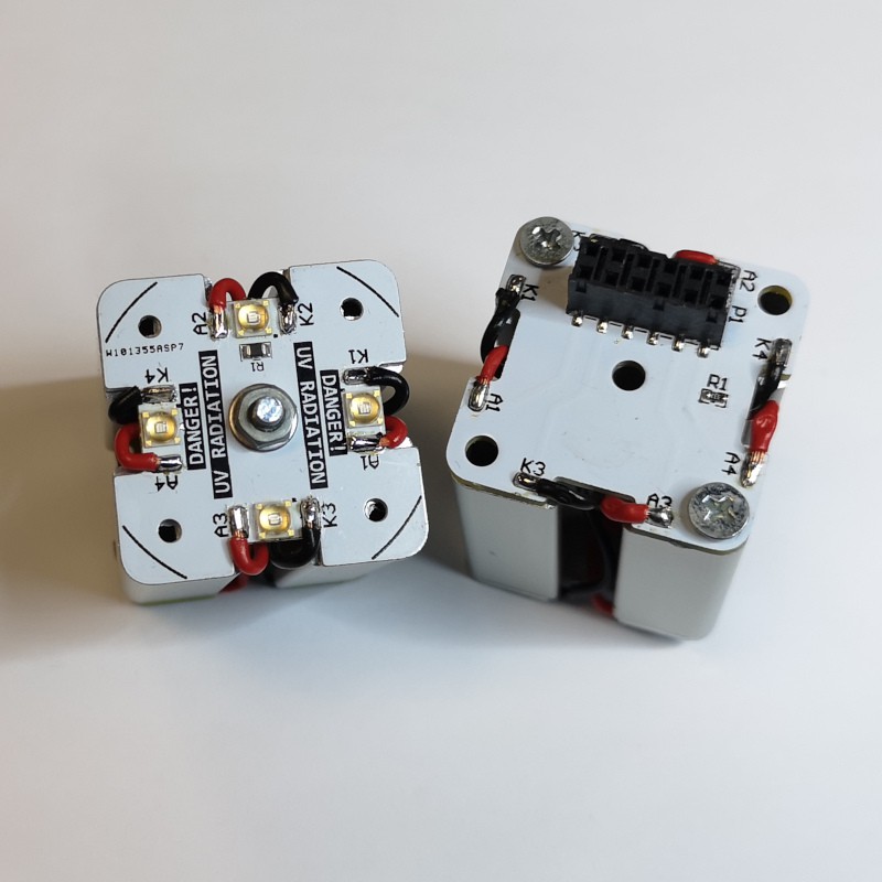
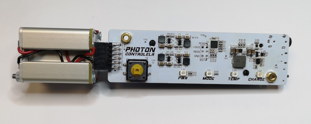
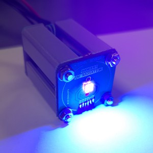
Loctite EQ CL32 is available in two versions. 365nm and 405nm. The reason is that there are UV adhesives that are sensitive to different wavelengths of light. Major drawback to this is that you have to buy both devices to have both light sources. My approach to this is modular. I will have a replaceable LED module that plugs into a universal controller module with Li-ion battery. This means that having a device that supports both wavelengths will be cheap and compact.

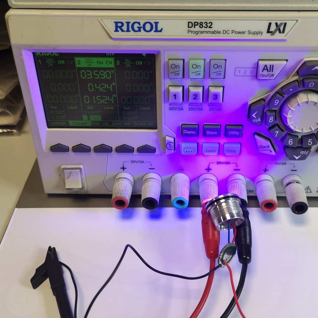
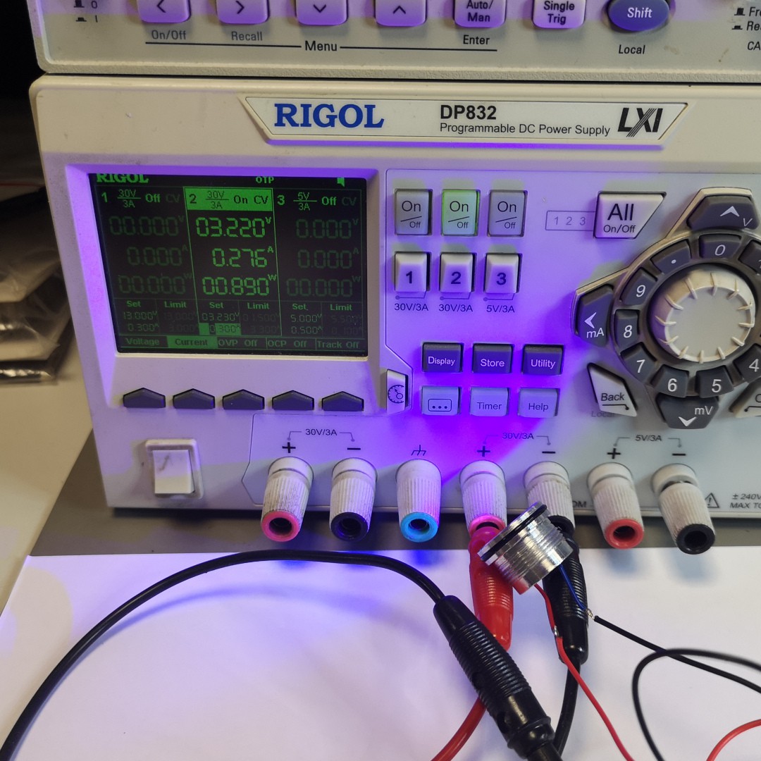
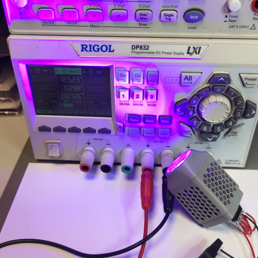
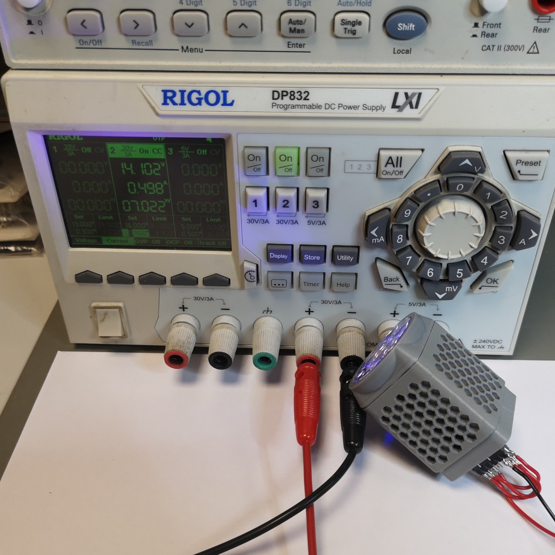
IRRADIATED POWER OF 100 mW/cm² OR MORE

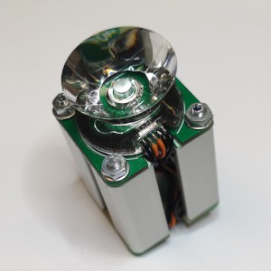
According to documentation, most popular UV adhesives like LOCTITE AA 3525, 3526, 3491, 3494 require about 100 mW/cm² of irradiated power to successfully cure in a reasonable amount of time. Array of LEDs that is used (PQ2N-3FLE-AFC & LTPL-C034UVD365) is more than capable of radiating that amount of power. To concentrate radiated power into smaller surface areas and increase efficiency lenses are used (CA13546_EMILY-RS & C12285_ANGIE-S).

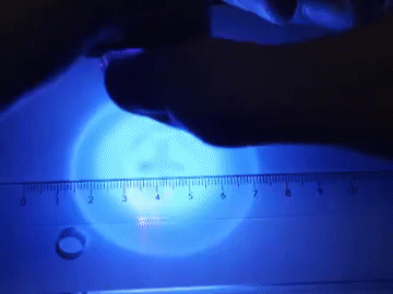
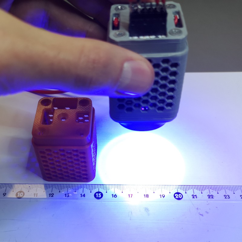
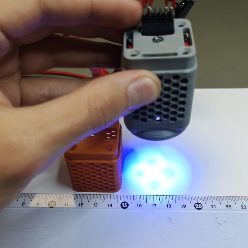
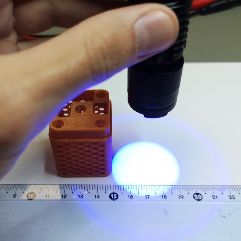
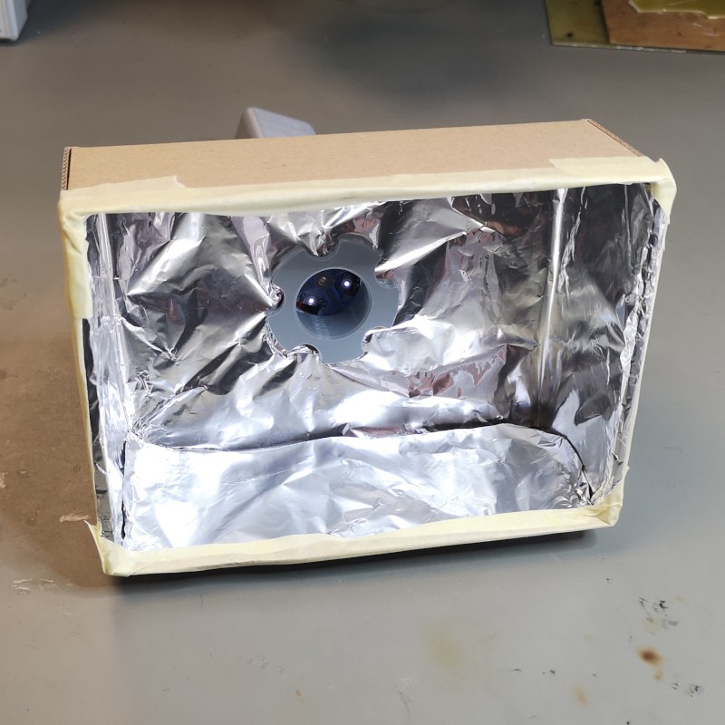
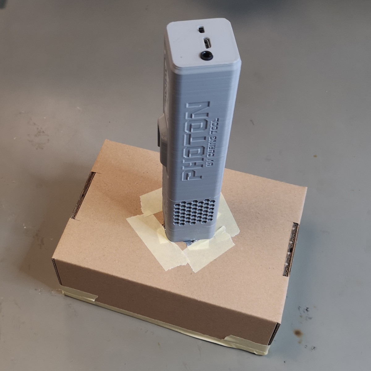
This demonstration shows effect of CA13546_EMILY-RS lens on PQ2N 400nm module. At height of around 10cm lens focuses light into circle of around 4cm, while central hotspot, where radiation is highest is around 2cm.

LICENSE:
PHOTON UV Curing Tool (c) by Mile

PHOTON UV Curing Tool is...
Read more »

PHOTON_Documentation.zip

Documentation for Photon Prototype

x-zip-compressed - 6.80 MB - 10/04/2020 at 20:48

Download

  • Photon vs. Regular UV flashlight

    Mile10/20/2020 at 21:43 0 comments

    One question that comes up alot is: “Why would you use this tool for UV curing, when you can use 5$ UV flashlight from eBay?”. Let's take an empirical approach to that question.

    Pictured below is a 5$ UV flashlight. It has an aluminium case, adjustable lens and accepts a single Li-ion AA battery. Led with a heatsink and a driver board is also shown.

    If the LED module is connected to 3.6V(nominal voltage of a single li-ion cell) it draws 420mA or 1.5W of power. Measuring voltage on LED diode with voltmeter shows forward voltage of 3.23V. When LED is powered with that voltage, it draws 270mA or 900mW of power. That means that the driver circuit has efficiency of 60% with above input parameters. If we assume 30% efficiency of wire bonded 3535 LED, that flashlight has radiometric power of 270mW.

    For comparison, PQ2N LEDs of Photon 400nm LED module consume 3.7W of power. With assumed efficiency of 45%(refer to datasheet) for CSP LEDs we get radiometric power of 1670mW. On the other hand LTPL-C034 LEDs on 365nm LED module consume 7W of power. With assumed efficiency of 30%(refer to datasheet) for wire bonded 3535 LEDs we get radiometric power of 2100mW.

    If we take a look at technical documentation for LOCTITE AA 3494 light-cure instant adhesive we can see a plotted graph that shows cure time vs. depth of cure when irradiated with a light source of 50 mW/cm² and 100 mW/cm². It is obvious that a light source with higher power density is needed to reduce cure time and to cure thicker layers of adhesive.

    To estimate power density we need to measure illuminated surface area first. It is measured from a height of 5cm(typical object curing height) and then divided by total radiometric power value. For 5$ flashlight average power density of 21.5 mW/cm² is estimated, for 400nm LED module 59 mW/cm² and for 365nm LED module 107 mW/cm² respectively.

    *5$ flashlight does not have a reflector so a good amount of light is wasted. This is indicated by large circles of light outside the central light spot shown on image above. Adjustable lens functions more like a collimator.

    **Since Photon LED modules have temperature sensors, initial LED current can be increased to achieve higher radiometric power levels since most curing applications take less than 5 minutes. For continuous illumination above stated power levels are maintained.

    ***Those 5$ UV flashlights are modified "regular flashlights". The reason why they are not most optimal choice for UV curing is that they are designed to house one(single die) LED.

    CONCLUSION: 5$ Flashlight is good enough for curing thin layers of UV adhesives but not suitable for larger surfaces or thicker layers of encapsulating compounds. Considering Photon has higher output power, built in battery charger, support for external triggering, is open source and has material cost of 40$ or less it looks like a logical choice for people that use UV curing products on a regular basis. Especially considering that a professional equivalent like CL32 costs around 1000$. 

  • Finishing Photon Prototype

    Mile10/05/2020 at 07:33 0 comments

    Here is video that showcases finished prototype. Although prototype is finished there is room for improvements. Some road map of future development and updates:

    • Adding more functionality to firmware with more user options.
    • Adding features like "Quick Charge" for faster battery charging and USB bootloader for easier configuration of the device by user.
    • Optimisation of BOM and PCB design for cheaper production.
    • Improving design and ergonomics of enclosures.
    • Improving project documentation with user manual.

  • Economics

    Mile10/04/2020 at 19:47 0 comments

    From the economic side, material cost of controller module is around 20$, 365nm LED module 20$ and 15$ for 400nm LED module. There should be also considered 5$ per set(Controller + LED module) for automatic assembly(pnp) and production testing.

    Good news is that with more modules being produced the price of material will fall. Good estimation would be 30-50% on quantities of more than 100. 

    Rundown of components needed is provided in BOM. Future wise there are also savings possible with regard to component choice. Example being pricey Semtec "SSM-106-F-DV" connectors and Keystone 1042 battery holders.

    If a larger quantity of modules are needed, to optimise the process PCBs can be panelized. Replacing TH components with SMD versions would also reduce manufacturing time and cost since they can be placed by PnP machine and eliminates soldering by hand by human worker. Here is example of panel with V-cut, industrial edge and fiducial markings for PnP and Stencil printers.

    On the PCB there are also Test Points. Test points are used to automate PCB testing and verification. If simple "bed of nail" test jigs are used, cost of manufacture and lead times can be short short. Here is picture of onboard test points for generic 50mil pogo pins and simple test jig that I made for different project. Similar system can be used for testing on this project.

  • Photon - Features

    Mile10/04/2020 at 19:13 0 comments

    Here is closer look at some interesting features of Photon prototype:

    LED Box Adapter:

    Sometimes directed light isn't needed. Instead what is needed is illumination of large surface area. That is where this adapter comes in. It is basically simple bolt and nut design. The idea is to use cardboard box lined with reflective material(like aluminum foil) to achieve effect of so called "light box". This approach is used when illumination of larger surface area is needed. Reflective foil reflects UV rays to object where instead they would be wasted.

    UV Filter:

    Since long UV exposure is harmful, a way to protect the operator of this device is needed. That is why this protective filter was designed. It's just plain orange plexiglass sheet. The reason why this works is because the sheet blocks all wavelengths except orange(620nm). This won't be useful against strong directed light like laser but it will be more than enough for reflected UV rays from illuminated surface. Yellow or red plexiglass can also be used. Here is simple demonstration of effectiveness of this simple filter. Fluorescent residue on PCB is conformal coating used to protect PCB from corrosion.

  • Prototype Assembly 2/2

    Mile10/04/2020 at 18:25 0 comments

    This is last project log regarding prototype assembly. So, to complete one Photon device you need:

    • Assembled LED modules
    • Controller electronics module
    • 3D printed enclosure files(project repository)
    • 2 x DIN912 M3x25mm screws
    • 4 x DIN965 M3x45mm screws
    • 4 x 6x2mm disc magnets
    • Cut to size plexiglass sheet(red, orange or yellow)

    And pictures of assembled device:

  • 3D Design Files

    Mile10/04/2020 at 17:53 0 comments

    Enclosure was designed to allow easy swapping of different LED modules. Design itself is easily 3D printed on home FDM printers. Main parts are:

    • Power switch, charging input and external trigger connector located at the back of the enclosure.
    • Embossed markings for power, mode, temperature safety and charging indication.
    • Big and ergonomic tactile switch for turning on the LEDs.
    • Magnetic UV filter to protect operator from reflected UV radiation.
    • Push-in mount for mounting the device. Push-in GoPro mount adapter available.
    • Easy to disassemble enclosure with two fasteners for easy access.

    3D model of complete assembly is available in the project repository. There are also ready to print .stl files. Here are some renders of the new prototype enclosure.

  • Prototype Assembly 1/2

    Mile10/02/2020 at 20:39 0 comments

    After the initial concept, a fully functional prototype has been made. Some functionality that has been added:

    • LED Driver circuit that supports performance 365nm and economy 400nm LED module.
    • Automatic recognition between different LED modules.
    • Temperature protection of LED modules.
    • Automatic power adjustment of LED modules that depends on their temperature.
    • USB Rechargeable and user replaceable 18650 Li-Ion battery.
    • Different modes of operation(continuous and momentary illumination).
    • Externally triggered for use with an external controller.
    • Aluminium substrate PCBs for better thermals.

    All above mentioned improvements are documented in project schematics. Schematics include LED module PCB, Controller PCB and Connector PCB. Schematics are also available in higher resolution(.pdf) in the project repository. Special care was taken to reduce the number of unique components to make the assembly process more economical.

    To make the assembly process easier and faster assembly drawings were generated. They are also available in .pdf format.

    And finally here are some pictures of assembled modules. White colour of the solder mask was chosen because it is more reflective than the default green. This will help in reflecting UV radiation of LEDs outward.

    After assembling LED modules I did some testing. Since I am now using aluminum substrate PCBs I should have much better thermals. As it can be seen on the picture from thermal camera, temperatures are around 5°C lower, but what is more important is that there much better heat transfer to aluminum heatsink. This picture was taken after 30 minutes of operation so there is some "thermal lag" for heatsink to reach set temperature. This allows driving of LEDs at even higher power levels to achieve higher output power in shorter time periods.

  • Measuring thermal performance

    Mile08/31/2020 at 11:18 0 comments

    As mentioned above some thermal issues were discovered on LED modules, so I decided to take a closer look with a thermal camera. Out of two modules 400nm one looks worse since LEDs are packed so close together. The main problem is as I see it that pcb does not conduct heat to heatsink. Specific thermal conductivity for FR4 is around 0.3W/mK, while depending on substrate for ALU PCBs is in the range of 2-4W/mK. Making new versions on ALU PCBs will solve the issue. I might also consider arranging(spacing out) LEDs to improve thermals further.

    *Left: PQ2N-400nm module Right: LTPL-365nm module.

    Image below shows the detailed construction of the LED module. You can see thermal conductive pad(greenish stuff) and thermistor wrapped in kapton between it and PCB.

  • Testing of LED modules

    Mile08/31/2020 at 06:55 0 comments

    After assembly I decided to do a practical test of LED modules. Plan was to test the curing of TP-2500 adhesive and PCB solder mask. TP-2500 is OCA type adhesive and is used to bond surfaces where maximum light transmissions are needed. It is very popular in the phone repair business. It is used to glue the front protective glass to the LCD. PCB solder mask is also a generic one that you would use during PCB repair or manufacturing process. Since these products are very popular they are good benchmarks.

    Video shows me using a 365nm(LTPL-C034UVD365) LED module. Testing with a 400nm(PQ2N-3FLE-AFC) module gave similar results. Both modules were running at lower power values than designed(about -30%) due to heat dissipation problems caused by having FR4 PCB. Final version should have aluminium substrate PCBs which will increase output power and curing performance.

    *For testing purposes "Mechanic" brand of UV adhesive and solder mask was used.

  • Designing and making LED modules

    Mile08/31/2020 at 05:48 0 comments

    Pictured below is a removable LED module. It is designed to be easily 3D printed on any hobbyist 3D printer. To increase airflow, a mesh pattern was incorporated into the design.

    *Fully assembled LED module inside and outside of 3D printed enclosure.

    REMOVABLE LED MODULE IS MADE OUT OF:

    1. PCB with array of LEDs, either PCB with array of LEDs, either with PQ2N-3FLE-AFC or LTPL-C034UVD365.
    2. PCB with connector to interface with main controller module.
    3. Aluminium extrusion heatsink.
    4. Thermal transfer compound between PCB and heatsink.
    5. Thermistor to monitor LED temperature.
    6. Lens with lens holder.
    7. Fixing screw.

    *Pictured are two different LED modules during assembly process. One is without enclosure.

View all 11 project logs

Enjoy this project?

Share

Discussions

Davinder Chandhok wrote 12/07/2020 at 12:12 point

When will this project be available for purchase? (It seems from your wording that you intend to manufacture it in larger scales?)

  Are you sure? yes | no

Similar Projects

Does this project spark your interest?

Become a member to follow this project and never miss any updates