Over the weekend I thought a bit about what I want to achieve, what matters most, what I'm not so interested in doing, and drew up a list of requirements to help me balance various design choices. It's in the description above. It will still evolve over time but it's still helpful to have a reference written down.
I also thought a bit about architecture. In order to support multiple processes on a 6502 you pretty much need address translation, otherwise they all have to share the same stack space at 0100-01FF. It's possible to do that (GeckOS does when running on the C64) and I think it's also possible to do it in a safe "protected" way, but it's not very elegant. My goal is to explore the benefits of hardware support anyway. Using memory paging and address translation is more in line with how larger real-world architectures work.
So I thought a bit about how to organise that, what addressing scheme to use, and drew some diagrams on paper. These are horrible to read, but they make sense to me and I wanted to share them anyway. When things are more concrete I'll make some clearer one electronically.
The first is just brainstorming the addressing scheme:
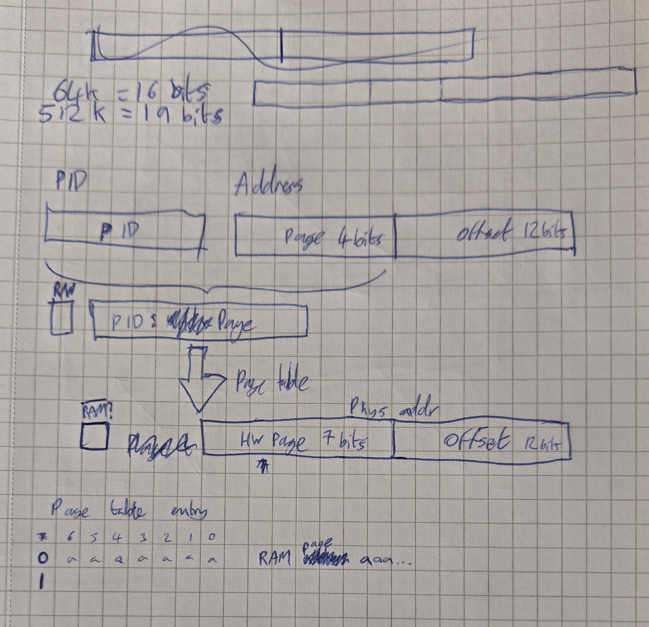
I've ordered a 512K RAM chip, that needs 19 address bits. The CPU's address space is 16 bits. I'm going to take the top few bits off that and use them combined with a process ID (and maybe the read vs write bit) to look up the top bits of a physical address in a separate RAM chip. I'm using 8-bit memory (16-bit was expensive) so I don't have many bits to play with in the result. I'll reserve the top bit to flag non-RAM access, as eventually I'd like to allow that kind of thing to be mapped as well. So I have seven bits left that can form the top seven bits of the physical RAM address.
The 512K RAM needs 19 address bits, so there are 12 left. That means my page size needs to be 12 bits, leaving 4 bits at the top end to select which page. It divides the address space into 16 chunks of 4K.
I wasn't very happy with this, I'd prefer to have more, smaller pages. Also this doesn't leave room in the page table output for any restriction bits, e.g. read-only. But I want to keep things reasonably simple at first. Later on I could add a second RAM chip to get 16 bits of data per page table entry; or I could sequentially read the page table. But let's not overcomplicate things yet.
4K pages are also quite common if you look at other people's similar systems, like André's. He used a dedicated MMU chip that outputs 12 bits rather than 8, which seems handy, but it's discontinued. He used the higher bits to store access rights. Expanding to 16 bits per PT entry is very appealing now.
Next up, I sketched how the system should look to a user process. It's fairly simple:
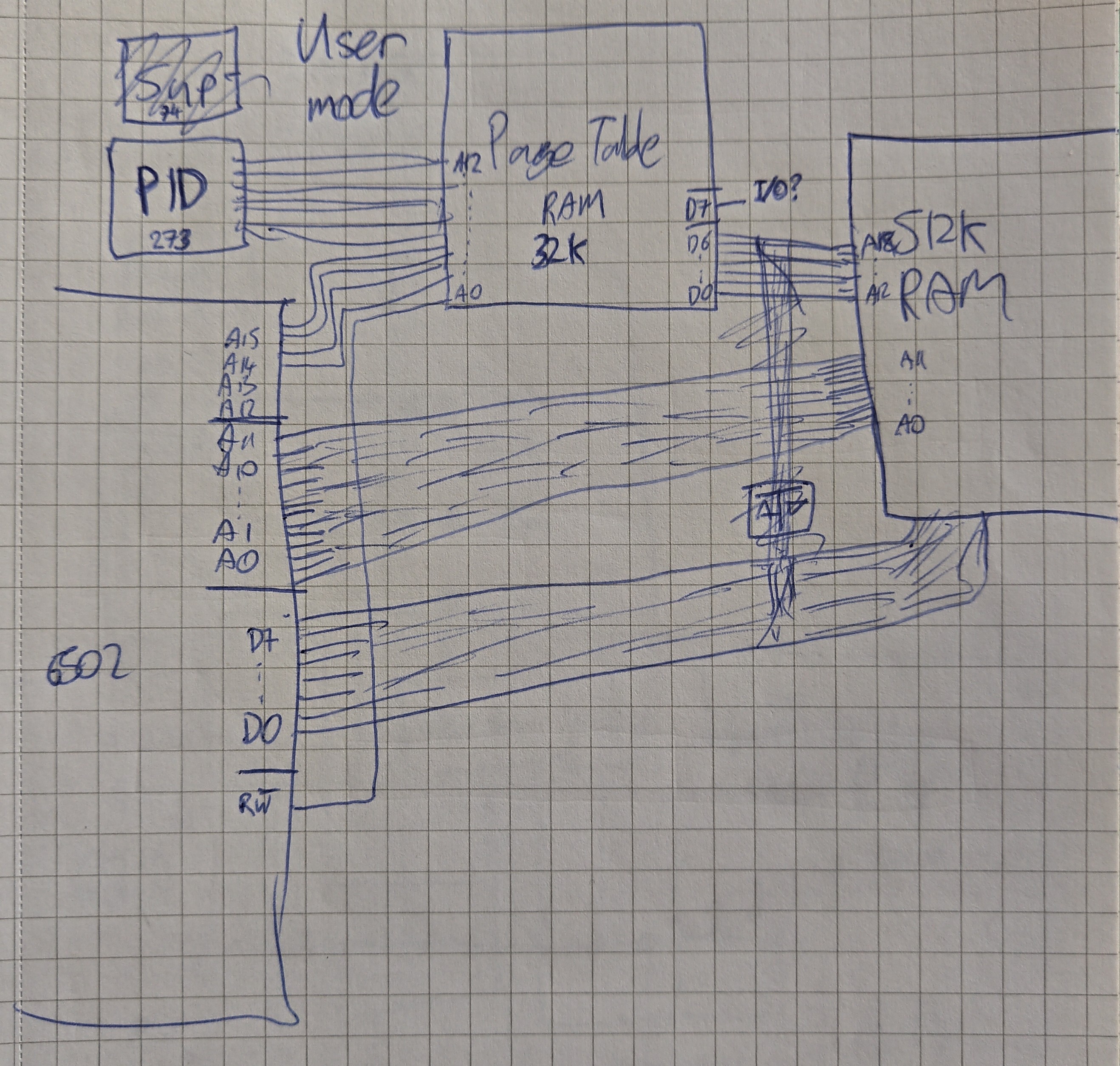
I wanted the whole 16-bit address space to be usable, I didn't want some of it wasted on ROM or I/O mappings that the user process isn't allowed to use anyway. That should all be opt-in.
Note also the '273 register in the to left - this stores the process ID (PID), which also feeds into the page table (PT).
The user mode process doesn't have access to read our write either the PID or the PT entries. Ignore the link to the data bus on the right hand side, I started adding the links needed in supervisor mode, but then decided to draw a separate diagram for that:
So... wow, this got complicated fast.
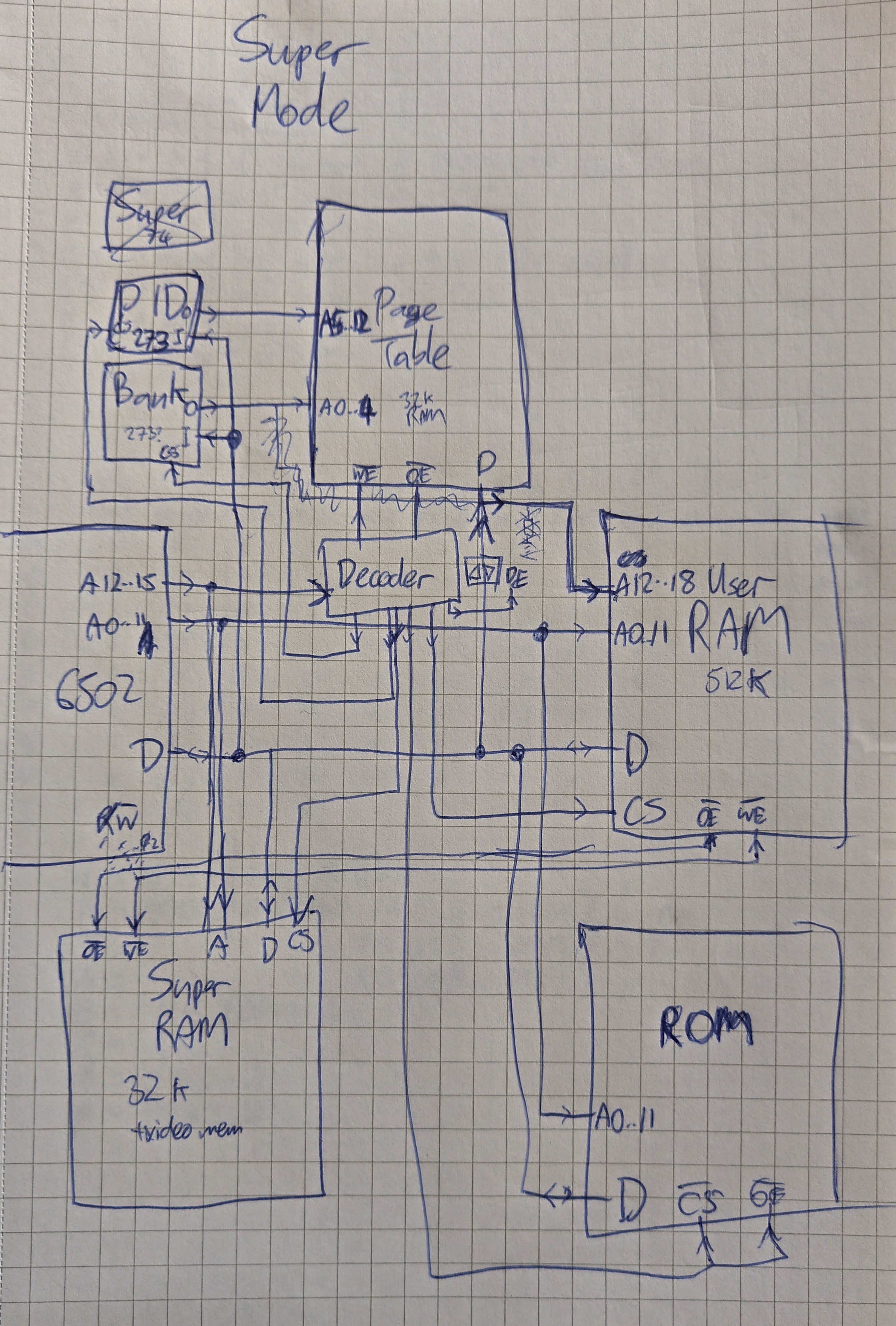
In the lower right there's a ROM, which is where the supervisor code lives. There also an extra RAM in the lower left. This is maybe optional... But I'll likely be implementing this in a system that uses shared RAM for video memory, and that's where that lives at the moment. It could also be where the supervisor stores all it's own data. In that sense, from the supervisor's perspective, the whole thing is more like a regular computer but with user RAM and the page table added in like peripherals. I thought this was an interesting way to look at it.
The supervisor needs to be able to write to the user RAM anyway, so to do that it needs to also be able to send arbitrary inputs to the PT. It can't just use A12-A15 because it's using those for regular address decoding. So there's an extra "bank" register which it can program to control the PT.
In order to update the PT, there's a link from the data bus to the PT output (it's data pins) with a bus transceiver to control whether the data bus or PT is outputting. The data bus is also wired to the PID and Bank registers, and a decoder decides which of these things should be active at any time based mostly on A12-A15.
I would have liked the decoder to be driven based on the PT's output. This may be necessary in the end, to allow user processes to access more than just user RAM. However, writing to the PT itself is something that depends on that decoding, and we can't read from and write to the PT simultaneously, as it's not dual-ported. Maybe it should be, or maybe I can access it twice per clock, latching the write and performing it when phi2 goes low again. Something to figure out in the future!
This sketch is obviously not complete, but it's a good start. Next I thought a bit about the decoder logic, but I'll post a separate update about that...
Discussions
Become a Hackaday.io Member
Create an account to leave a comment. Already have an account? Log In.