Regarding the decoder, it felt like a really good fit for the PLDs that Dawid Buchwald had been recommending recently, so I thought a bit about how that logic works. What does the supervisor need to be able to do? How can it set up the various control lines to achieve it? How many outputs does the decoder need? Here the resulting logic table:

The letters at the side correspond to various types of operation listed above. The signals driving the chips are along the top of the table. The Greek letters are unique outputs from the decoder, as some of the columns are constant or identical to each other. It seems a pretty good fit for a simple PLD, but what about user mode, what's different there?
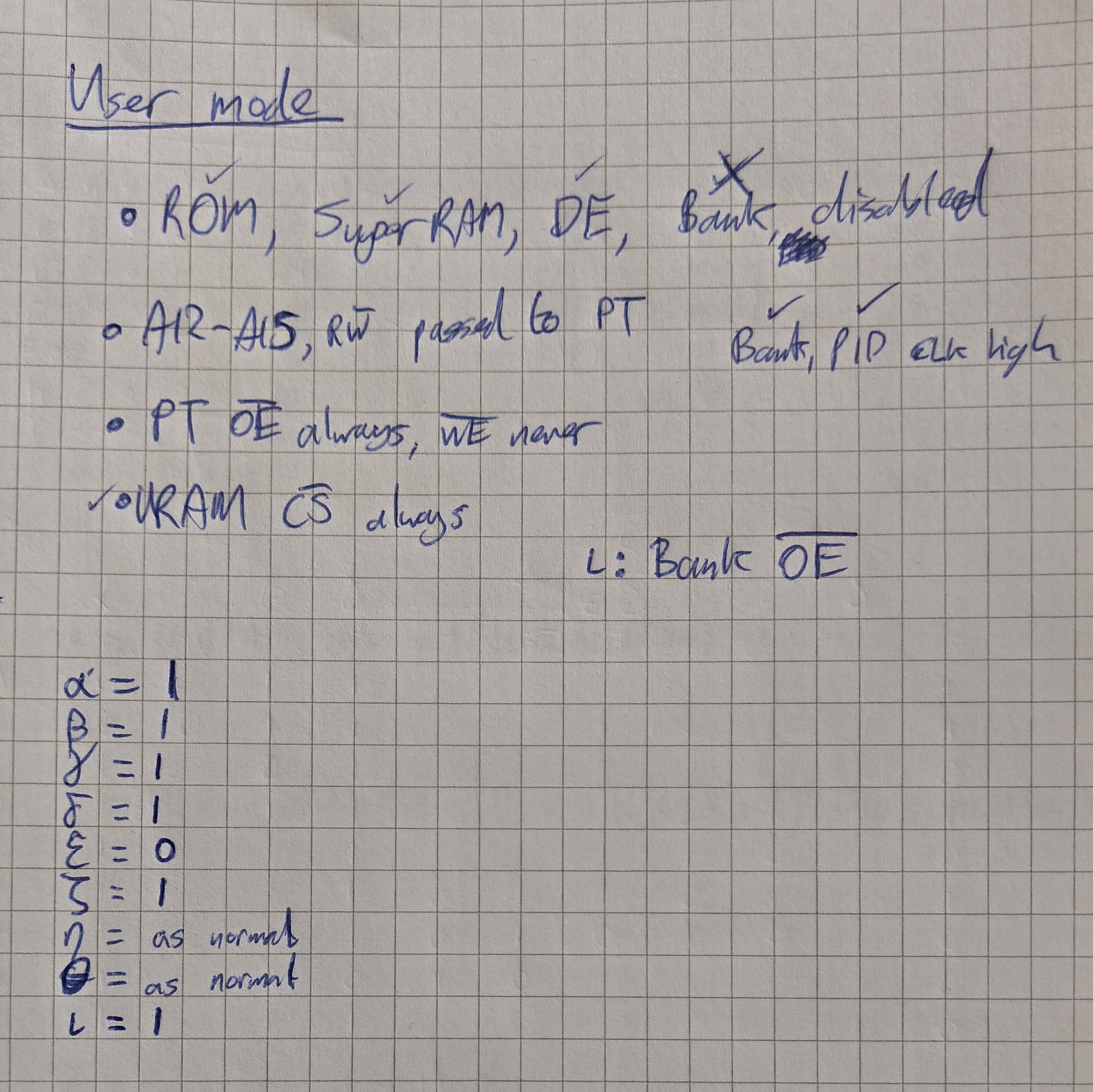
Hmm, mostly just constant values in user mode. But the bank register needs another control line here, designated iota. But it's actually exactly the same as "are we in user mode?" so not really necessary as a decoder output.
Maybe eta and theta could be dropped if I'm running low on outputs and want to put other logic in here later. They don't have much in common with the other outputs. I've considered using the spare space in this PLD to implement the Super/User flag.
I also wondered whether I could implement the bank register entirely in a PLD. As it stands I'd need a bus transceiver to gate the CPU's A12-A15 and RW lines, as well as a '273 or similar for the register. Or maybe a multiplexer. But can a small PLD serve both purposes?
It would need five bits of registered outputs to store the value in, and five inputs for A12-A15 and RW to pass through in user mode. But I don't think it would be possible to use the registered outputs to drive the page table in user mode, as they are clocked and it would be hard to clock the new data in at the right point in the cycle. So I'd need another five outputs to actually go to the PT, and I'd make them get set to either the register values (in super mode) or passthrough of the CPU address (in user mode). That's now ten outputs. I also need another five inputs from the data bus in super mode, and also the super/user flag... that's eleven inputs... More than is supported by these chips. 🙁
It's close enough that I think there must be a way to make it fit. Maybe using the address bus instead of the data bus to set the value.. the code wouldn't be pleasant though. There are also other considerations, like the logic for when to go into or out of super mode, and it's possible that I just need to spread some of this logic across several PLDs to get a tidy result overall. Something to come back to later!
Discussions
Become a Hackaday.io Member
Create an account to leave a comment. Already have an account? Log In.