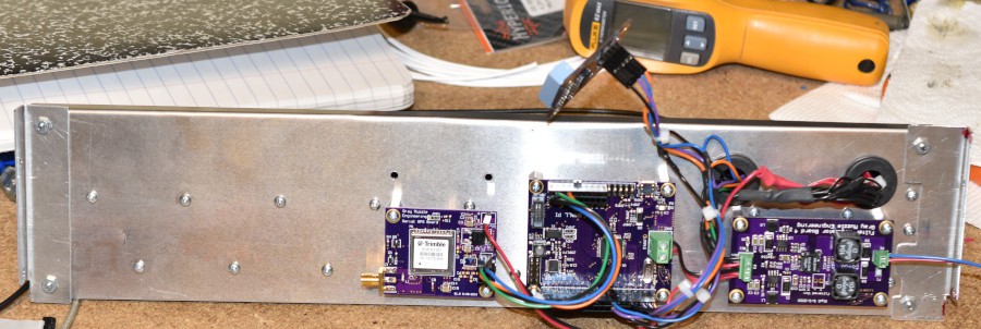
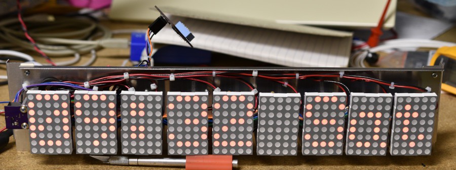
This project re-uses a few boards from previous projects and adds a couple of new ones. Some software ties everything together.
Existing boards:
LED Matrix Driver boards. On the front side of the chassis.
SmallPi SAMD21J18 controller board. The middle board on the back side of the chassis.
GPS Receiver board. The leftmost board on the back side of the chassis.

New Boards:
Ambient Light Sensor board. Lives next to the leftmost display module on the front of the chassis.
DIP Switch board. Visible sticking up on the wiring harness.
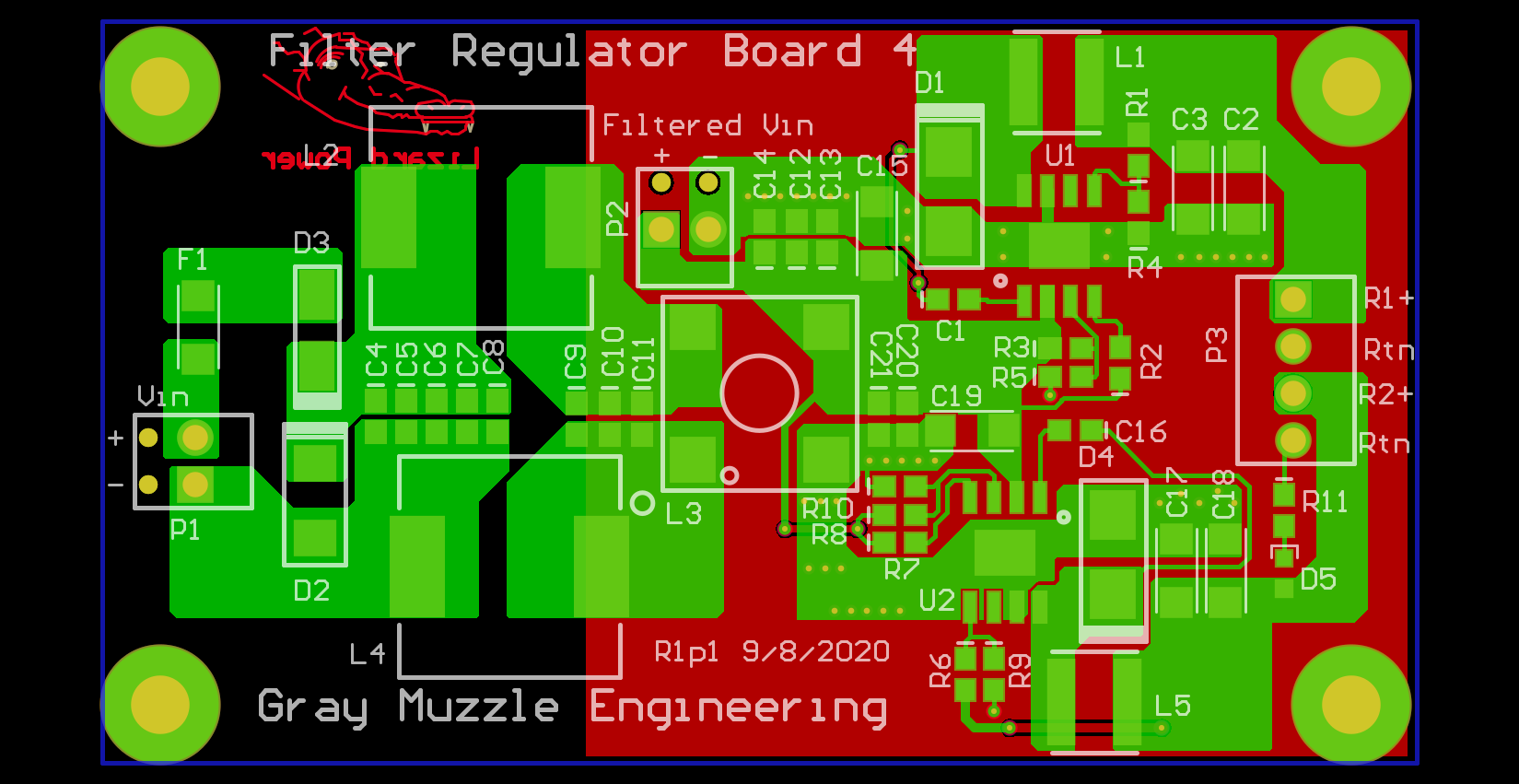
Input power filter/regulator board. The rightmost board on the back side of the chassis.

Communication with the LED Matrix modules is via an I2Cbus. There are 18 devices on this bus, so it can get pretty busy at times. It clocks at 400KBPS and the bus is spread out over about 18" of wire. I was a little concerned about this many devices that are spread out over this much distance, but it looks reasonable on an O'scope and I don't see any signs of data errors in operation. The ambient light sensor and the DIP switch are also read over an I2C bus. A different bus was used for these two just to separate them from the display module traffic.
When I started the project, I thought about developing all of the firmware for the project on my desktop machine and then porting it over to a microcontroller when all the features were implemented. This is why I chose to put the DIP switches on the I2C bus (with a TCA9534 I/O Expander chip). It is also why I picked an Ambient Light sensor module with an on-board ADC (BH1726NUC-E2). In the end, I decided it was not worth the effort on a project this size to take this approach and just did the development on the SAMD21J18 part.
Communication with the GPS receiver is done with a UART. It is running at 4800baud which is the "standard" for NMEA traffic.
A serial debug console connection is also available. This will mostly be used to see what the GPS reciever is doing. The Copernicus II seems to be a pretty generic GPS receiver. The sensitivity is OK but not outstanding. I suspect that running this in our wood framed house with asphalt shingles may be marginal for getting a fix unless it has a window view. Time (and the debug port) will tell on this one.
The SAMD21 family uses something they call Sercom modules to support UART, I2C and SPI communication. I wanted to run 4 of them for the communications described above. The SAMD21E18 only has 3 of those modules accessible, so that drove the choice to use the SAMD21J18 based board.
I started using the Copernicus II modules in another application several years ago. I had most of the software to parse and control these modules left over from that. It still took some work to add parsing for a couple of additional messages and control over a couple of aspects of the receiver. Also, the original code was developed to run in a lot fatter environment, so there was a lot of error handling and parsing of marginally useful stuff that needed cleaning up.
All timekeeping is done in the GPS receiver. The firmware that is running on the SAMD21 parses the NMEA messages from the receiver, converts the "Time of Week" output value to local time and day of week, and formats it for display. I thought a lot about doing the timekeeping in the SAMD21 processor and disciplining it from the GPS data. If the GPS fixes inside my house prove to be intermittant, I will implement the local timekeeping, but I wanted to see whether this idea would work.
Time is extracted from the NMEA messages from the "Time of Week" parameter. "Time of Week" is the number of seconds since midnight on Saturday night, in GPS time. GPS time differs from UTC time by a varying amount. When this was written, UTC time lags GPS time by 18 seconds. The lag is referred to as GPS Leap Seconds, and the exact number is available in one of the proprietary Trimble messages. That value is subtracted from the GPS time to get UTC time. Converting the UTC time of week to local "time of week" is a simple subtraction of the time zone offset in seconds from the GPS "Time of Week" value.
Five bits of the 8 bit DIP switch data are sign exended into a 32 bit 2's complement number to provide the local time offset in integer hours. Also controlled by the DIP switch setting are:
12/24 Hour time display format.
Red / Green display color.
GPS receiver "High Sensitivity Enable".
The ambient light sensor is read once per second. The 16 bit value from the sensor is truncated to 8 bits and then checked against empirically derived thresholds to select the display driver current. At this time, there are 5 thresholds and that seems to be enough. The brightness steps are pretty visible on the display and if the project is running on a bench power supply, make a large difference in the power supply current.
Running the display at the highest current setting for red or green results in about 650mA at 3.3V into the displays. It is possible to run both the red and green which will give a yellow display and up to 1.3A of current into the displays. I opted to offer red or green only in the software. The display current fluctuates somewhat based on what characters are displayed. The I2C bus for the displays operates at the input voltage for the driver chips, and the microcontroller wants a 3.3V I2C bus. It would have been possible to configure the address translator chips on each module to level shift the bus, but since this project was designed from the bottom up, the display modules were already designed before this ocurred to me. Running the displays on 3.3V as opposed to 5V reduces the heat generated in the display drivers some, and the displays seem to run fine on 3.3V.
The one irritation of running the displays at 3.3V is that the power filter/regulator boards that I have already designed are configured to supply higher current at 5V and low current at 3.3V. The processor board and the GPS board both have an LDO regulator on them so they want 5V input to the regulators. The GPS and processor boards need less than 100mA between them, so my existing filter / regulator boards would not work to drive this project. A new filter regulator board was designed and laid out with two switching regulators running from the filtered input power. Either regulator output voltage can be configured independently and either regulator can supply up to 2 Amps. There is a lot of filtering on the input side of the regulators. I want to experiment with these input filters to see how effective they are in blocking the conducted emissions from the two switching regulators.
There is some debate about the use of multiple parallel capacitors of different values in filters. The parasitic inductance of capacitors mean that large capacitors that are capable of supplying the instantaneous current demands stop looking like capacitors at disappointingly low frequencies. Electrolytic capacitors are really bad in this respect, but the ceramic chip caps suffer from it as well. Lower value capacitors have lower parasitic inductance, so they continue to behave like capacitors to higher frequencies, but won't supply much energy. The most obvious solution to this is to put some smaller value chip caps in parallel with the high value caps in the expectation that the high value caps will supply the instantaneous current while the low value caps will provide low AC impedance to higher frequencies. I have seen several competent people claiming that this idea does not work. I have also heard some people claiming that it does work. I want to see for myself, so the input filter design used here has sites for a range of capacitors.
The design for the filter and regulators came from an earlier iteration of a filter/regulator board that had an LDO regulator driven off the switching regulator to provide the 3.3V output. It had much lower current capabilities. In a night of insomnia, I took the schematic for the original board and removed the LDO and copied the switching regulator for a second independent voltage. I remembered to replace the switching regulator inductors with higher current parts, but forgot to do that with the 3 inductors in the input power filter. The board layout was completed and sent out to OSH Park. A few nights later, I remembered this and started digging around for suitable higher current inductors. It turns out that the existing PCB layout could hold suitable inductors after scraping a lot of solder mask off. When I do PCB layout for power projects, I use a lot of poured polygons rather than individual traces. This saved my hide on this project.

The rev 1 boards came in yesterday and I built one up this morning. Since the new inductors are large enough to cover the old footprints, it does not even look totally awful. It is a little crowded around the filters though. I sent the rev 1.1 boards to OSH Park last night.
On the topic of emissions, I have not done any checking on emissions for this project yet. My suspicion is that the LED drivers are going to radiate quite a bit and I hope that the input filter will block any conducted emissions from going out on the cable to the wall wart that will power this project. The project will be packaged in an aluminum case with the power supply, processor board and GPS receiver in a closed off part of the case. An antenna cable for the GPS will come through the case with the antenna on top of the case. The displays will be exposed to the front. I want to spend some time measuring the EMI for my own knowledge and also, since I am an amateur radio operator, I don't want to radiate a bunch of noise into an already noisey neighborhood.
 Bharbour