 Christoph
Bud describes the compensation procedure in his project's details (see here: https://hackaday.io/project/169390-a-10x-100mhz-differential-probe/details), and the description is good, but it doesn't provide any scope shots of the process. To compensate the probe, you need a square wave signal at two different voltages. I used my bench PSU, an IRLML6344 (NFET) and a 1k resistor for that. The FET's gate is driven by my scope's square wave output.
Step 1: cancel DC common mode error
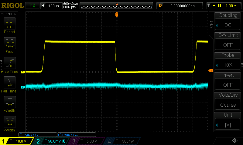
Set the PSU to 20 V to get a 20 V square wave on the FET's drain. Connect both probe inputs (+ and -) to the FET's drain. You'll see something like this:
(Ch1 is the 20 V square wave, Ch2 is the probe's output).
We want the flat parts of Ch2 (left and right of the plot's center) to end up on the same level, by adjusting R11. The result:
Step 2: match positive signal path AC gain to DC gain
Lower the square wave voltage to 2 V and connect probe + to drain, probe - to gnd:
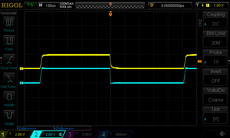
The goal now is to get rid of that little overshoot at the top of the rising edge by adjusting C5. We want the top and bottom to be as flat as possible. If you can't do that with C5, change C7 to move the trim cap to the right range.
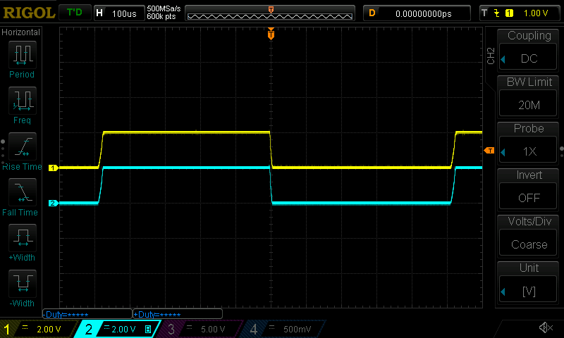
Result:
Step 3: match AC gain between positive and negative signal paths
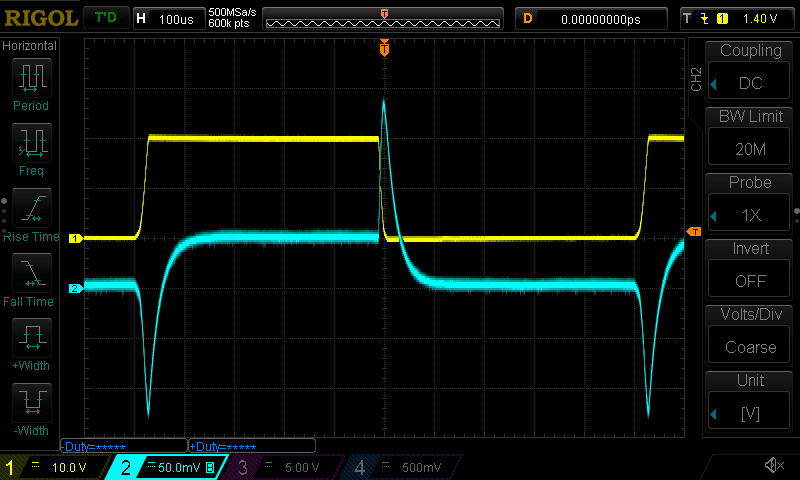
Back to a 20 V square wave, both inputs connected to the FET's drain:
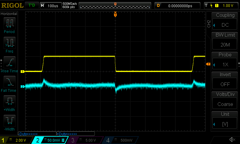
Those peaks will now be removed by adjusting C10.
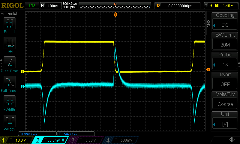
Result:
It's not perfect, but the probe reacts to just about anything in its surroundings.
That's it. The whole procedure took about 10 minutes.
Discussions
Become a Hackaday.io Member
Create an account to leave a comment. Already have an account? Log In.