 DIY GUY Chris
Hey guys! I Hope you already enjoyed my previous post about "Bluetooth AT Commands Settings" and you are ready for a new one, as usual I made this tutorial to guide you step by step while you make your own PCB business card since I find it as an amazing project that combines both electronics learning and PCB designing and it could be a good start for beginners to upgrade them making skills.
During the making of this project, we tried to make sure that this post will be the best guide for you in order to help you if you want to make your own PCB Business Card, so we hope that this post contains the needed documents.
This project is so handy to make specially after getting the customized printed circuit boards that we’ve ordered from JLCPCB to improve the appearance of our Business Crad and also there is enough documents and codes in this guide to allow you create your beautiful business card.
We've made this project in just 2 days only, just one day to get all the needed parts and finish the hardware making and the assemble, then one day to prepare the code to suit our project.
What you will learn from this project :
- Making the right hardware selection.
- Prepare the circuit diagram to connect all the choosen components.
- Create the appropriate PCB design.
- Solder the electronic parts to the PCB.
- Start the first test and validate the project.
Step 1: Circuit Diagram

As always guys, I try all the time to pick up some good and easy electronics projects and the first step in our project is the Circuit Diagram that will be transformed to a PCB design.
In order to prepare the schematic I used EasyEDA design tool which is a super handy for both beginners and professional PCB designers, it has a built-in simulator for signal measurment and a very well developed library where you can find all the needed components for your circuit design with them appropriate footprint.
Our circuit is a basic one, it has a USB connector for power supply and a ATMega328 microcontroller where we will connect five RGB LEDs which are controlled by three push buttons, all the components here are SMD parts except the USB connector which is a through hole part.
Step 2: PCB Making


After tracing the tracks you will have the full schematic ready to be transformed into a PCB design.
Just clicking on transforming to PCB design and all what we need now is setting the PCB outline to set the Business card size.
Size of the board is so important to fit in people pockets and wallets so I took the measurements of an existing badge which has the same standard dimensions of a business card 54.75mm x 85.50mm
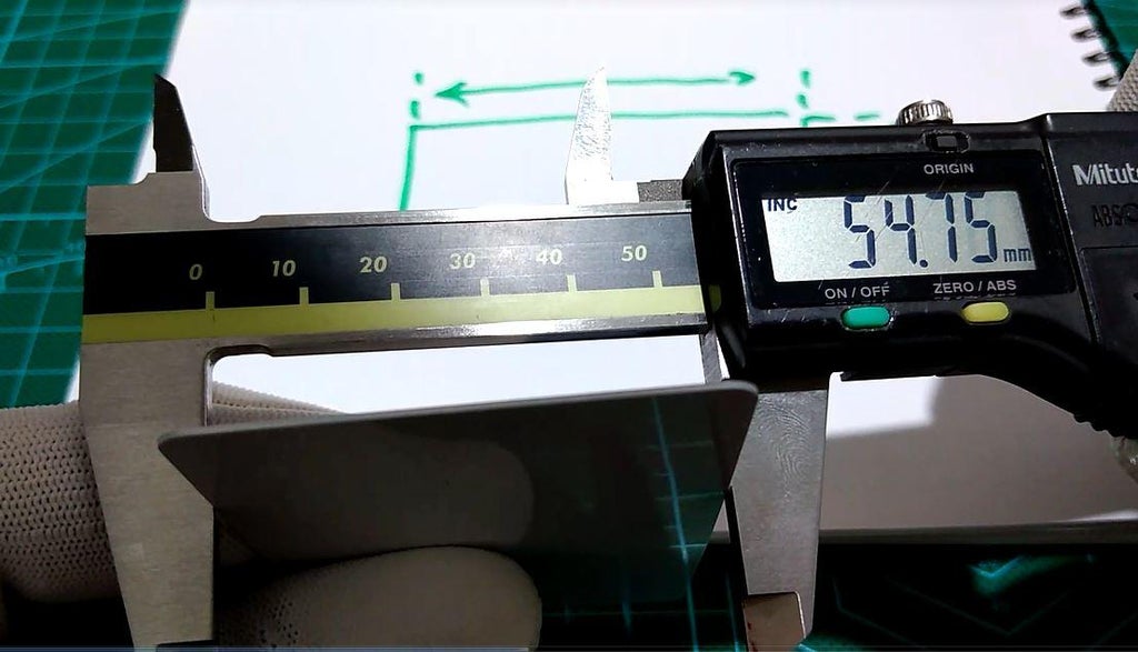

then I get back to EasyEDA design tool to create the board outline that follows the measured dimensions.
Now we drag and drop the components in the board layout and we start writing the personal information like the full name, the job, the address and contacts as silkscreen layer.
After adding some cool logos and icons the board is ready for routing and all what it takes is routing these components, in order to have my name written in golden finish material (ENIG) I set it as top solder mask layer but be careful while routing this board you should avoid the contact of two tracks of two different nets with the top solder mask pattern or it will be shorted.
Step 3: PCB Manufacturing Settings


Now our design is ready for production so all what we need is generating the GERBER files and drop them to JLCPCB for ordering, just set some PCB production settings like the PCB color which is black or you can choose whatever available color you like and the ENIG surface finish to have the golden look and the PCB thickness is set to 0.4mm to give it the appearance of a real business card.
I ordered 50 pieces of this board as trial and I dropped it into production with some other PCB designs to get them all shipped in one order pack
Just four days to wait and I got my PCBs well...
Read more »


 Jefferson Bueno
 ElectroBoy
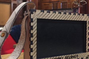
 Michael Delaney
Looking for opportunities to boost the company's competitiveness? Our 24/7 live chat support is a trusted partner in this endeavor. Our inbound and outbound traffic strategies modify your market process and optimize your revenues. Your trustworthy new and repeated customs resource will be an outsourcing call center for companies such as ours. Concentrate and allow us to call upon you to improve your company.