Please see my "first project" on how to setup everything:
https://hackaday.io/project/175642-a-first-fpga-project-spi
I used an Intel MAX10 FPGA (10M08SAE144C8G), and then a ATMEGA256RFR2 to interface with the FPGA over SPI. The ATMEGA256RFR2 is 3.3 V, so compatible with the FPGA.
For this project, I created a SPI interface on the FPGA. The ATMEGA256RFR2 is the master. Since this is my FPGA, and maybe we could move away from the "slave" term, I called the FPGA the "sidekick".
Anyway, I also added a "register map" to the FPGA. This version has 8 indepedent PWMs, all running at 32 bit, and 50 MHz. I tried to comment the heck out of the code. This is a complete project, so future versions could have more features.
Enjoy!
The PWM period can be from 50 ns all the way up to ~86 seconds. The PWM on time can be as short as 25 ns. Not bad! :)
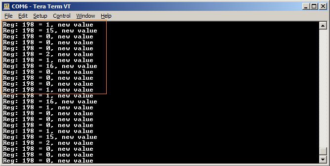
Below is the teraterm session between the PC and the ATMEGA256RFR2. Register (decimal) 198 is the SPI register for output (i.e., UDR0). Not show, I set the chip select pin to 0 (from 1). Then, I enter 1 to edit a register. Then, address "15". Next, I set the 32 bit register to 2 (i.e. the period of the PWM is 2 ticks of the 50 MHz FPGA clock). Then, I write 1 to register 16 (i.e, for the PWM to be high for 1 tick of the 50 MHz FPGA). I highlighted the session in orange...
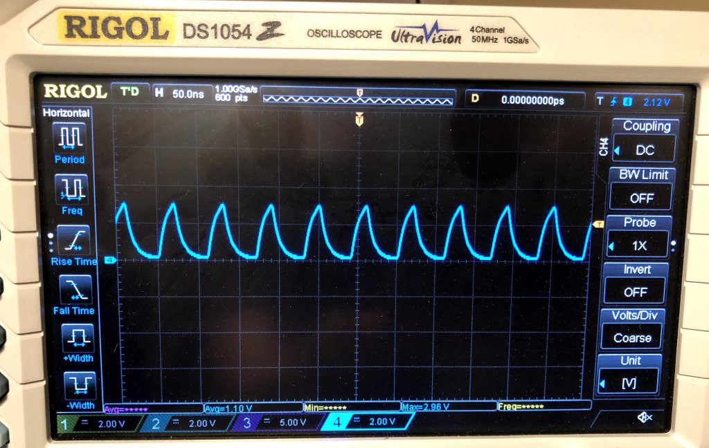
This gave rise to the super short PWM output on pin 41 of the FPGA (i.e., one tick of the 50 MHz clock, and a period of two ticks of the 50 MHz clock):
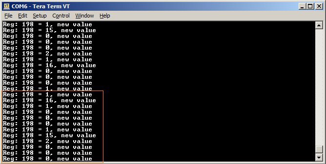
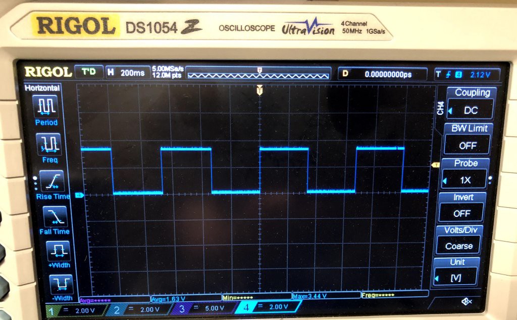
Next, I programmed in larger values for the PWM settings (i.e., the programmed values for the 32 bit register were decimal 1, 0, 0, 0 which will mean an actual decimal value of 16777216 ticks for the PWM output to be high, or 336 ms high), and a period of 33554432 ticks (or 671 ms).
And voila!
For interest, here is the Quartus report:
Flow Status Successful - Sun Nov 01 22:36:01 2020
Quartus Prime Version 20.1.0 Build 711 06/05/2020 SJ Lite Edition
Revision Name spi_pwm_micro_test
Top-level Entity Name spi_pwm_micro_test
Family MAX 10
Device 10M08SAE144C8G
Timing Models Final
Total logic elements 1,628 / 8,064 ( 20 % )
Total registers 923
Total pins 18 / 101 ( 18 % )
Total virtual pins 0
Total memory bits 0 / 387,072 ( 0 % )
Embedded Multiplier 9-bit elements 0 / 48 ( 0 % )
Total PLLs 0 / 1 ( 0 % )
UFM blocks 0 / 1 ( 0 % )
ADC blocks 0 / 1 ( 0 % )
 Justin R.
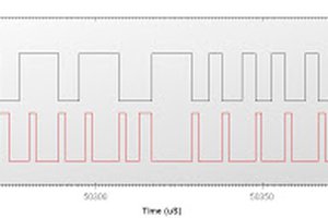
 BDM
BDM
 Dilshan Jayakody