The old adage that "you get what you pay for" certainly applies here. A highly integrated solution with simple control schemes poses limitations that aren't easily fixed.
Secondary regulation. The reasons for this have already been discussed and aren't a controller problem per se (any topology will exhibit) but one of coupling between the windings (i.e. leakage inductance). While a well built inductor will minimize this it won't achieve 1% (TI's demonstration boards using commercially built inductors are 10%). Hence, the secondary should be used to power circuits that can tolerate lose regulation.
Conditional stability. This is a result of the complex interaction of V2's low impedance with the control loop and current limit scheme. It is similar to the right half-plane zero found flyback boost converters. The events I've observed to induce this are:
- Vin droops below UVLO and then recovers to some operating value within a few volts of Vin_min (drops that do not go below Vin_min to not induce)
- High capacitive load on V2
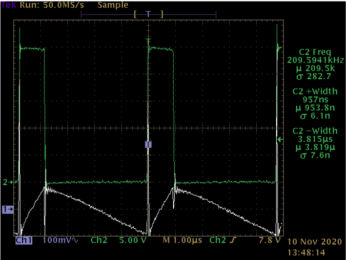
Both happen when the secondary is loaded and the primary output is lightly loaded (~>20%) or open. The switching node will go from a stable pattern:
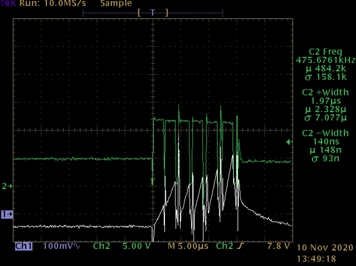
To one of bursts followed by a long off-time:
CH1 is the AC ripple component on the feedback (FB) pin which is necessary for stable operation.
The secondary output voltage will drop to some fraction of its rated output but the primary voltage stays close to its regulated value. If a specific minimum load is applied to the primary, or the secondary load is removed & then reapplied, the controller will resume stable operation. This condition does not occur if both outputs are open or only the primary is loaded (any value). It also does not occur in the opposite direction (sudden increase in Vin).
When the controller encounters these situations it begins by switching with minimum off-time (expected). After a few switching events, current has built-up in the inductor, trips the over-current circuit, and switching terminates. By this time the FB voltage is at or above Vref since V1 is not loaded. Several mS pass (I have measured +20) before the FB voltage drops below Vref and switching resumes. But energy in the secondary is gone so the process repeats. Crucial to this is the lack of synthetic ripple (AC component) on FB pin: it isn't generated due to the short off-times and already high voltage on the FB pin; it doesn't occur during 'cold starts' because the FB voltage is zero.
There is no easy way to fix this. Decreasing R4 to increase the ripple feedback will reduce the V1 load threshold but will not eliminate the instability. A simple hack is to add a diode across the outputs to pull V2 down. A more complex one is to add a synthetic ripple (mabe just voltage sense?) circuit to the secondary and couple to the feedback pin with a resistive summing circuit. Both require a non-isolated secondary.
I decided that the juice isn't worth the squeeze and instead tested the thresholds (Vin drop, minimum V1 load) necessary to avoid this condition (V1 load of ~ 60mA).
Current limit scheme. This is a hazard and likely failure mode when V2 encounters a short or over-current condition with a high input voltage. The specific conditions are: secondary is under load and encounters a short, the primary can be loaded or open, and Vin is high (for my tests 25V).
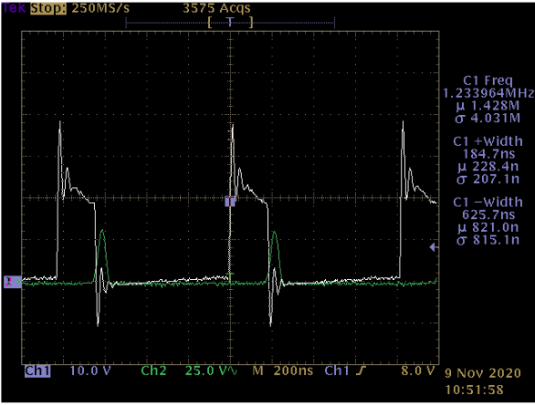
The controller uses a heuristic scheme to extend the off-time to limit the output current and provide a 'soft' foldback. A key determinant of the off time is the voltage at the feedback pin: the lower it is, the longer the off time. When the secondary shorts, the FB pin voltage remains close to its regulated value (2V) because the V1 output is fine (even when 100% load) and so the off time is short. The next switching cycle begins but is quickly terminated for over-current. The switching cycle looks like this:
The high secondary current (<800mA - well beyond rated 200mA output), combined with the high Fsw sends the controller and rectifer D2 temps through the roof in a matter of seconds. I recorded case temps of 177C for the controller and 184C for D2. Of course this condition does not occur if V1 is shorted (regardless of V2's loading).
I ran a destructive test of this condition to see what would fail first and after 5 minutes, amazingly, neither did. The controller would over-temp, shutdown, and after a few seconds turn back on to repeat the sequence. It was like watching a flashing stop light on the IR camera.
I am sure that one or both would eventually fail. My concerns are fire hazard and that the primary switch fails closed and destroys everything downstream of the supply (a typical failure mode of MOSFETs). A fused crowbar circuit would solve for this.
This is really a crappy control scheme and I'm not sure why TI did this. I've worked with some of their integrated direct-off-line controllers and under these conditions they simply shutdown & reset: they never get out of soft start so there's little current, almost no thermal stress, and certainly no risk of damage to the supply.
Provided V2 doesn't need isolation, the diode across V1/2 idea for instability solves this problem too. Otherwise, a possible solution is to add an external over-current protection circuit; or accept the limitation but do destructive tests to make sure the failure modes are safe & acceptable for the application.
Conclusion. High ratio secondary windings create problems with solutions that can exceed the economic viability of the design. I suspect that this is why in all of TI's documentation and their eval boards the secondaries are 1:1. Use with caution.
Discussions
Become a Hackaday.io Member
Create an account to leave a comment. Already have an account? Log In.