 Mitsuru Yamada
1. Hardware
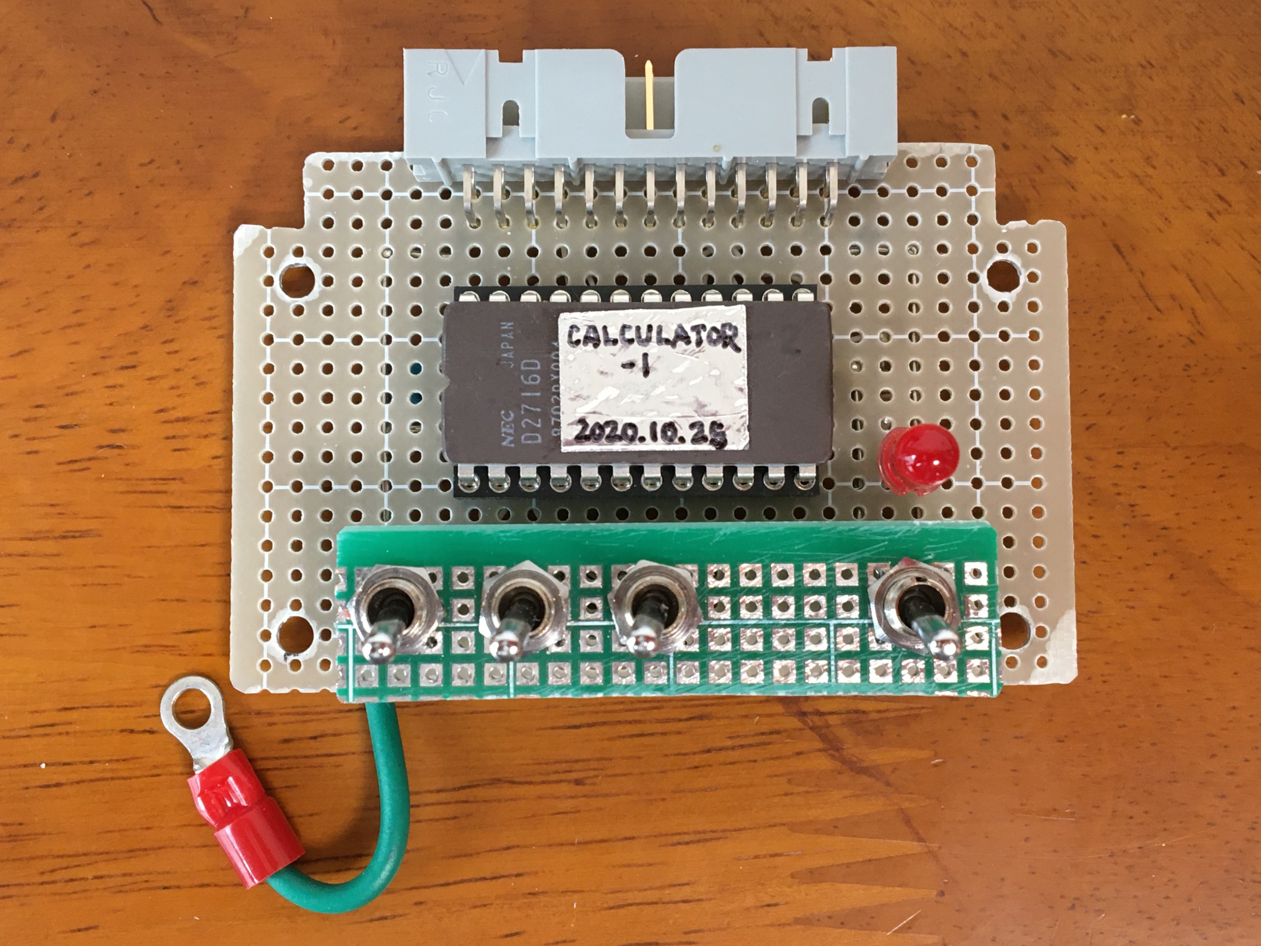
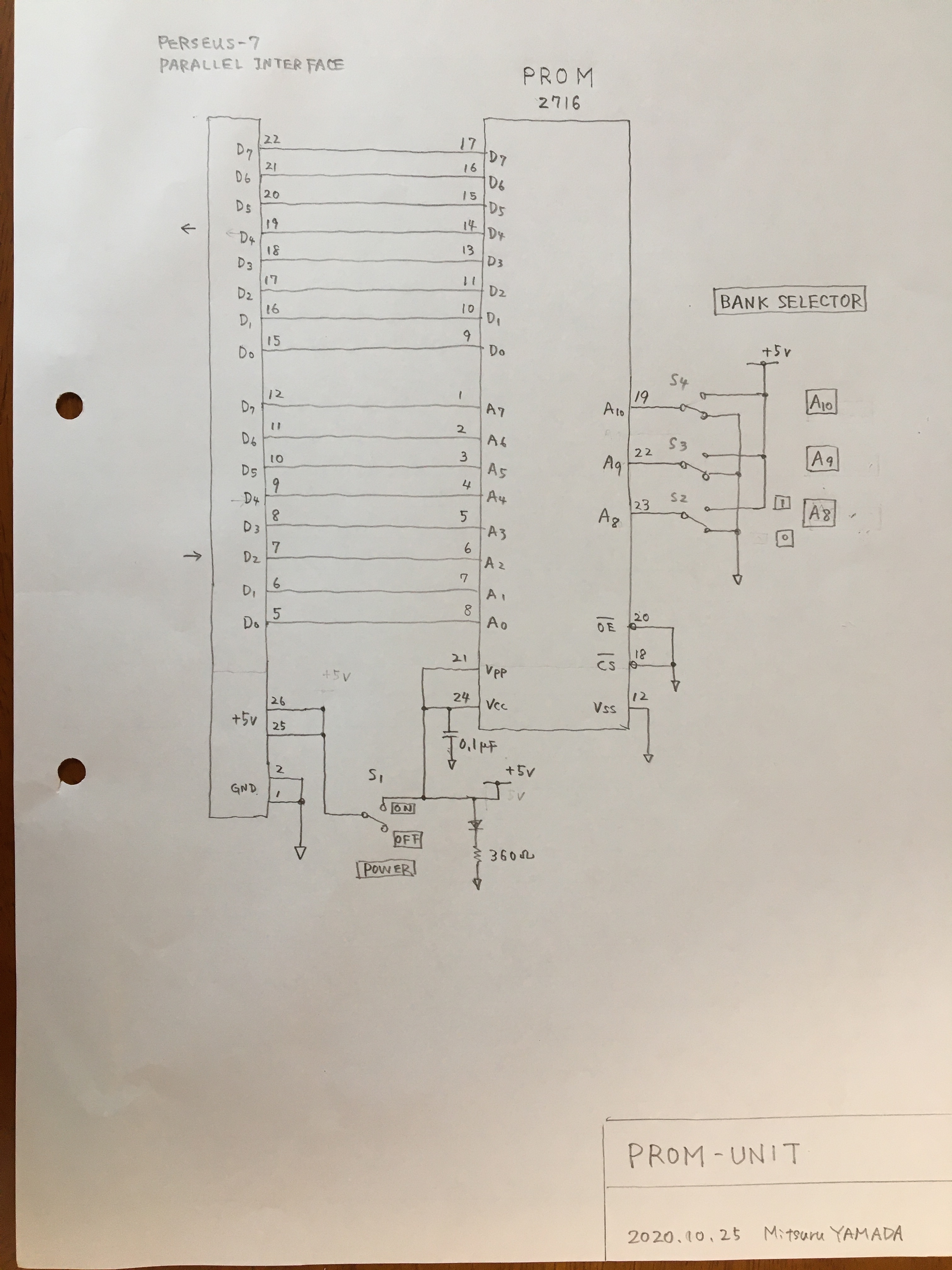
The circuit is very simple. As shown in the schematic, the 8 bit output of parallel interface is connected to an address input of the ROM. Since the 2716 has 11 bit address line, rest of 3 lines are connected to bank selector switches. An 8 bit of data output of the ROM is connected to the input of parallel interface. Since the chip select signal is not controlled and is always active, data is output just by adding an address. The housing is used a 12 cm x 9 cm x 3.5 cm aluminum die-cast box same as the numpad.
2. Software
As shown in the assembly code of the boot loader, the boot loader program outputs ROM addresses and inputs corresponded ROM data. Output address is incremented by X index register. Storing to a memory is used an indexed absolute addressing.
3. Result
I have made a 2 kbyte external ROM module with a size similar to a currently on the market 2 TB USB hard disk. Since the hardware has been simplified so that only 256 bytes can be loaded at one time. To load the 992 byte calculator software, it is necessary to set a bank of the module with the switches and execute it four times while changing the initial value of the destination address of the boot loader. I used my own ROM programmer to write the data to the ROM.
Reference: MM2716E 16,384-Bit(2048 x 8)UV Erasable PROM, National Semiconductor (datasheet)
Related articles:
https://hackaday.io/project/175924-fully-manual-prom-programmer
https://hackaday.io/project/175893-6502-computer-runs-calculator
 padnest
 SHAOS
SHAOS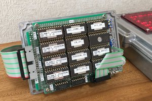